4. The DA14585/586 Hardware
The basic Development Kit consists of a single basic Board containing the DA14585/586 BLE SoC in QFN40 package. For the schematics and layout of the board in full detail, please refer to the respective documents on the portal.
4.1. The Basic Kit board
Figure 1 illustrates the physical layout of the Basic Kit board. The basic Kit board provides the necessary hardware to enable:
Full digital connectivity with external hardware using UART, SPI, GPIO, and I2C
USB based debugging capabilities using the SEGGER J-Link on-board debugger

Figure 1 The DA14585/586 Basic Kit
4.2. Configuring the Basic Kit Board by Jumper Settings
The DA14585/586 supports booting from UART. The jumper settings are displayed below:

Figure 2 The DA14585/586 Basic Kit Jumper Setting
Figure 3 shows the layout of the header jumper, J4.

Figure 3 Jumper 4 Layout
Note
Please notice that the signals connected on the DA14585/586 SoC are located on the left pins row of header J4 as shown in Figure 4.

Figure 4 Data direction of UART within J4
Note
UART connectivity is enabled by shorting header as presented in Figure 2.
UART connection between DA14585/586 and the MCU that provides communication over USB to a PC is realized through P0_4, P0_5 (for null mode), P0_6 and P0_7 (for full UART).
For DA14585, data flash through SPI connectivity is enabled with the jumper configuration which is presented in Figure 5. Please notice that for DA14586, this configuration is meaningless and it must be avoided. DA14586 SoC incorporates the flash internally (2Mbits).

Figure 5 DA14585/586 Boot from external SPI memory
4.3. Board Layout
The layout of the basic board is displayed in Figure 6.

Figure 6 DA14585/586 Basic Board layout
Components of Basic development kit:
U1: Dialog BLE SoC, DA14585 or DA14586 in QFN40 package. DCDC converter of SoC is configured in Buck mode. Two crystals are used, 16MHz and 32.768KHz.
U5 or U7: SPI data flash, MX25R2035. Two packages are available, U5 –WSON MX25R2035FM1IH0 and U7-SOIC8 - MX25R2035FZUIL0 – (default). For DA14586, flash memory is not mounted.
U4: MCU where Segger license is applied. UART and JTAG connectivity is provided to DA14585/586 SoC
SW1: Reset push button. By pressing the button, used can hardware reset the processor
J4: 28 pins header. Signal and power pins of DA14585/586 are provided. Also the interconnection between BLE processor and Segger license MCU for JTAG and UART is done through jumpers.
J5: 3 pins connector. DA14585/586 can be supplied by either 3.3V generated from on the development kit or by coin cell battery applied on the bottom side of the development kit.
J9: two pins header. It enables user LED. LED is driven from P1_0.
J10: 10 pins header. It is used for monitoring DA14585/586 port 2 pins.
J11: 10 pins header. Only P3_0 is provided on pin 1. Please notice that for DA14586, P3_0 is not used.
Note
The schematic diagrams, BOM, and Gerber files are illustrated in detail in the Development Kit Documentation.
4.4. Connecting the Basic Kit to the host PC
The Basic Kit includes an embedded J-Link debugger which allow easy communication with the development host over USB.
The DA14585/586 SoC is configured only in Buck mode on this development kit. A choice can be made between 3.3 V (via USB: J5 1-2) or VDD (a coin cell: J5 2-3). No battery is needed when running via the mini-USB cable.
Note
The basic Kit is connected to the host PC over the connector marked as USB (J3), as shown in Figure 6 using a standard mini-USB cable.
5. The DA14585/586 Hardware
The Pro Development Kit (ProDev Kit) consists of a motherboard (MB-PRO) and a daughterboard featuring the DA14585/586 SoC of the desired package, WLCSP34 or QFN40. .. _MB-PRO: https://support.dialog-semiconductor.com/system/files/resources/E-da14580devkt-p_vb_schematic.pdf .. daughterboard: https://support.dialog-semiconductor.com/system/files/resources/da14585_wcsp34_prodb_va1.pdf
5.1. The ProDev Kit Motherboard
Figure 7 illustrates the physical layout of the ProDev Kit motherboard. The daughter-board containing DA14585/586 device is shown in Figure 10.
The ProDev Kit Motherboard provides the necessary hardware to enable: * full digital connectivity with external hardware using UART, SPI, GPIO, and I2C * USB based debugging capabilities using the SEGGER J-Link on-board debugger * USB based UART communication with the host PC using a Future Technology Devices International (FTDI) chipset which converts UART to USB
Note
The DA14580 and the DA14585/586 share the same ProDev Kit motherboard (DA14580 DEVKT).
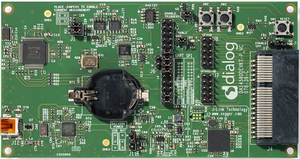
Figure 7 The DA14585/586 ProDev Kit Motherboard
5.2. Configuring the Pro Kit Board by Jumper Settings
The DA14585/586 supports booting from UART. The jumper settings are displayed below:

Figure 8 DA14585/586 Jumper Settings
Figure 9 shows the layout of the header jumper, J5.
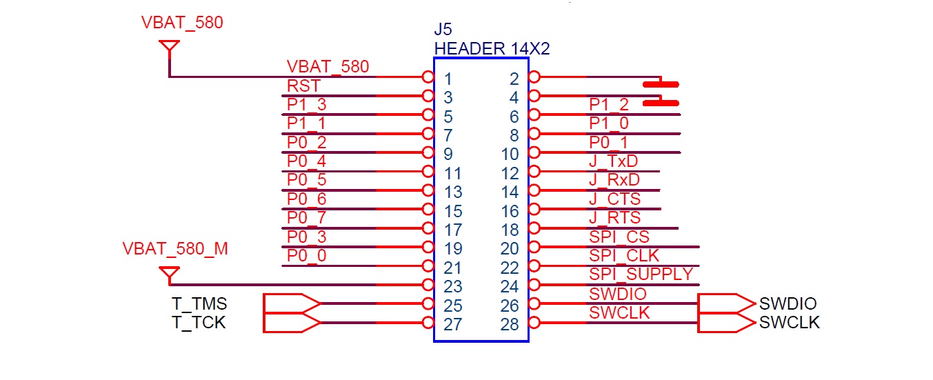
Figure 9 Jumper J5 Layout
5.3. Board Layout
The layout of the boards is displayed in Figure 10.
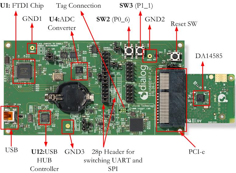
Figure 10 DA14585/586 Board Layout
Note
The schematic diagrams, BOM, and Gerber files are illustrated in detail in the Development Kit Documentation.
5.4. Connecting the ProDev Kit to the host PC
The ProDev Kit motherboard includes an embedded J-Link debugger and an FTDI chipset which allow easy communication with the development host over USB. Before connecting the ProDev Kit to the host PC, make sure that the motherboard and the desired daughterboard module are properly connected. A choice can be made between 3.3 V (via USB: J11 1-2) or VDD (a coin cell: J11 2-3). No battery is needed when running via the mini-USB cable.
Note
- The ProDev Kit is connected to the host PC over the connector
marked as USB (J12), as shown in Figure 10 using a standard mini-USB cable.
- When mounting a battery on the daughterboard, Jumper J11 should be removed.
For proper battery functionality, a small modification should be made. See the workaround in Appendix C.