7. UART Booting options
- The boot ROM code initially configures the DA1453x UART controller with the following parameters:
Bits: 8
No parity
1 stop bit
Baud rate: fixed at 115.2 Kbps for DA1453x
The protocol required to establish successful communication and to download the SW image into the RAM is shown in the next tables depending on the chip:
The protocol starts with the DA1453x UART TX pin that transmits
0x02(Start TX – STX).The external device is expected to answer with a 0x01 (Start of Header – SOH) byte followed by 2 more bytes (LEN_LSB, LEN_MSB), which define the length of the code to be downloaded (the first byte is the least significant, second the most significant).
The DA1453x answers with
0x06(ACK) if the 3 bytes have been received and SOH has been identified, or answers with0x15(NACK) if anything went wrong.

Figure 17 Boot Protocol
After Byte number 4, the connection has been successfully established and the SW code will start to be downloaded. The next N bytes are received and put into the RAM and start at address 0x07FC0000 as shown in Table 4. Boot sequence concludes upon receiving 0x06 (ACK) via URX. checksum is calculated by XORing each byte successively, starting from an initial value of 0x00. At the end, SYS_CTRL_REG is set to remap to address zero for RAM execution (SYS_CTRL_REG``[REMAP_ADR0] = ``0x2) and to initiate a software reset (SYS_CTRL_REG``[SW_RESET] = ``0x1).
Address |
Byte 3 (MSB) |
Byte 2 |
Byte 1 |
Byte 0 |
|---|---|---|---|---|
0x07FC0000 |
Code byte 3 |
Code byte 2 |
Code byte 1 |
Code byte 0 |
0x07FC0004 |
… |
… |
Code byte 5 |
Code byte 4 |
7.1. Booting from 1-wire UART
The one-wire UART boot capability is introduced due to the limited amount of the GPIOs. Since the
booting from UART protocol is a half-duplex, a single GPIO is used in DA1453x for the external
UART. The protocol is the same as for a two-wire UART booting except that the Booter SW need to
change the pin direction before sending or receiving information.
The bootloader of the DA1453x support a 1-wire UART interface on pin P0_5 or P0_3 which is option(step) 2 or option(step) 3 of the booting sequence. To boot from P0_3, connect the FTDI RX and TX via a 1K resistor and connect the RX side of FTDI to the P0_3 pin.
Hint
The 1K resistor exists in the motherboard, when using it there is no need to do that.
The jumper settings to use the 1-wire UART are as shown in Figure 18 and Figure 19. They are marked as a white box with a red outline. The jumpers are set to enable the 1-wire UART functionality along with SWD but not the Flash. Using flash and 1-wire UART is described in the coming sections.

Figure 18 Jumper Settings for 1-wire UART on DA14531 DevkitP

Figure 19 Jumper Settings for 1-wire UART on DA1453x DevkitP
- Booting on the 1-wire UART using the SmartSnippets™ Toolbox requires the following settings:
- Select your target from
Boardtab on top right side of the application: 
Figure 20 SmartSnippets™ Toolbox Settings
- Select your target from
Check the logs to confirm the firmware download and now the device will boot from 1-wire UART.

7.1.1. Programming Flash using 1-wire UART
The Flash memory connected over SPI to the DA1453x can be accessed over the 1-wire UART. The description below will explain how to program the firmware into the Flash memory. To boot from SPI Slave using the 1-wire UART, the jumper settings and the board setup are shown in Figure 22.

Figure 22 Jumper Settings 1-wire UART with SPI Flash (Default)

Figure 23 Jumper Settings 1-wire UART with SPI Flash (Default) (DA1453x DEvkitP)
Figure 24 UART/SPI Selection
Once you have these configurations, the following steps to connect/read/write/erase are like in Section 6.2.1 . The DA1453x bootloader is capable also of booting from a specific booting path (new SPI pin assignment). We simply need to use the configuration properly by applying it in the OTP header fields. An application can determine by using the OTP header fields which SPI pins the boot ROM should use for booting from external non-volatile memory. Consider the following example:
SPI-CLK: P0_4
SPI-CS: P0_8
SPI-MISO: P0_3
SPI-MOSI: P0_6
The OTP header breakdown on the 0x7F87FC8 and 0x7F87FCC addresses is presented in Section 6.3.
On address 0x7F87FC8 the application should program: 0x02FFABAA (1 wire UART)
On address 0x7F87FCC the application should program: 0x03060804
Hint
Boot from Specific SPI Port provides more details about Booting from Specific SPI port.

Figure 25 The OTP Header Burned with New Values
7.2. Booting from 2-wire UART
The bootloader of the DA1453x supports a 2-Wire UART interface on pin P0_0 and pin P0_1. The hardware and software setup are like 1-wire UART except for the jumper settings and board setup as shown in Figure 26 ,:numref:Jumper Settings for 2-wire UART (P0_0 and P0_1) (on DA1453x DevkitP) and Figure 28.

Figure 26 Jumper Settings for 2-wire UART (P0_0 and P0_1)

Figure 27 Jumper Settings for 2-wire UART (P0_0 and P0_1)
The configuration on SmartSnippets™ Toolbox for 2-wire UART is as follow

Figure 28 Board Setup for 2-wire UART
The jumper settings on the motherboard from J1 to the J2 header are as shown in Figure 21. The UTX (of the FTDI chip) is connected using a jumper cable to J2-P20 (P0_0/UART-Tx of the DA1453x) and URX (of the FTDI chip) is connected to J2-P21 (P0_1/UART-Rx of the DA1453x).
Using the Booter from the SmartSnippets™Toolbox, download the firmware and the DA1453x will boot from the 2-wire UART as per step 4 of the boot sequence.
7.2.1. Programming Flash using 2-wire UART
The Flash memory connected over SPI to the DA1453x can be accessed over the 2-wire UART. The description below will explain how to program the firmware into the Flash memory. To boot from SPI Slave using the 2-wire UART, the jumper settings and the board setup are shown in Figure 30 and Figure 29 . To boot from SPI Slave using the 2-wire UART needs a modification in the pin configuration due to the reason that the P0_0 is multiplexed between DA1453x-UART Tx and SPI slave MOSI. Due to this reason we modify the pin configuration in the following way as shown below.

Figure 29 SPI-Flash Pin Configuration on DA14531 DevkitP

Figure 30 SPI-Flash Pin Configuration on DA1453x DevkitP
SPI Flash Pin Config
MOSI (SPI_DO) - P0_5
CS (SPI_EN) - P0_6
MISO (SPI_DI) - P0_3
CLK (SPI_CLK) - P0_4
Configuring DA1453x UART for SPI Flash Access and OTP Burning of Secondary Bootloader
When 2 wire UART (UART_TX = P0_0 and UART_RX= P0_1) is used to access the SPI flash (assuming that the P0_0 is not of any SPI pins), the DA1453x secondary bootloader should be used to boot from a specific booting path (new SPI pin assignment). We simply need to burn it in the OTP.
Simplified SPI Flash Access Using 1-Wire UART (P0_5) on DA1453x
When the 1 wire UART (P0_5) is used to access the SPI flash, the secondary bootloader is no longer needed.
Enhanced SPI Flash Access with 1-Wire UART (P0_5) on DA1453x, Eliminating the Secondary Bootloader Requirement
When the P0_0 is used as one of any SPI pins, the 1 wire UART (P0_5) could be used to access the SPI flash and then the secondary bootloader is no longer needed.
DA1453x Configuration: 1-Wire UART and SPI Integration with OTP Header Setup
When the P0_0 is used as one of the SPI pins, and also as UART_TX the secondary bootloader is no longer needed. You simply need to program the OTP header on the 0x7F87FC8 and 0x7F87FCC addresses, consider for instance the following example:
SPI-CLK: P0_0
SPI-CS: P0_8
SPI-MISO: P0_3
SPI-MOSI: P0_6
On address 0x7F87FC8 the application should program: 0x00FFABAA (2 wire UART)
On address 0x7F87FCC the application should program: 0x03060800
Figure 31 Jumper config 2-wire UART with SPI Flash
Enabling SWD Interface in DA1453x: Application Code Configuration with SYS_CTRL_REG
The SWD interface is disabled when OTP is programmed on DA1453x. It is possible to re-enable SWD in your application code via the configuration script. You need to program 0x1A1 to the SYS_CTRL_REG (P0_2 / P0_10). If the Firmware burned in the OTP has the debugger enabled, then the SWD interface will be enabled from the application itself without explicitly burned the configuration script.
void SystemInit (void)

#endif
{
        SetBits16(SYS_CTRL_REG,DEBUGGER_ENABLE,1);
Refining SWD Interface Reactivation in DA1453x Application Code: A Systematic Approach
For application code mentioning the DEBUGGER_ENABLE bits in SYS_CTRL_REG as just writing 0x1A1 to this register in application code can result in unexpected behavior, especially as this will remap OTP at 0x00000000 when a reset is triggered.
- To write on this register first on
programmertab chooseOTPon left side bar chooseConfiguration Script: 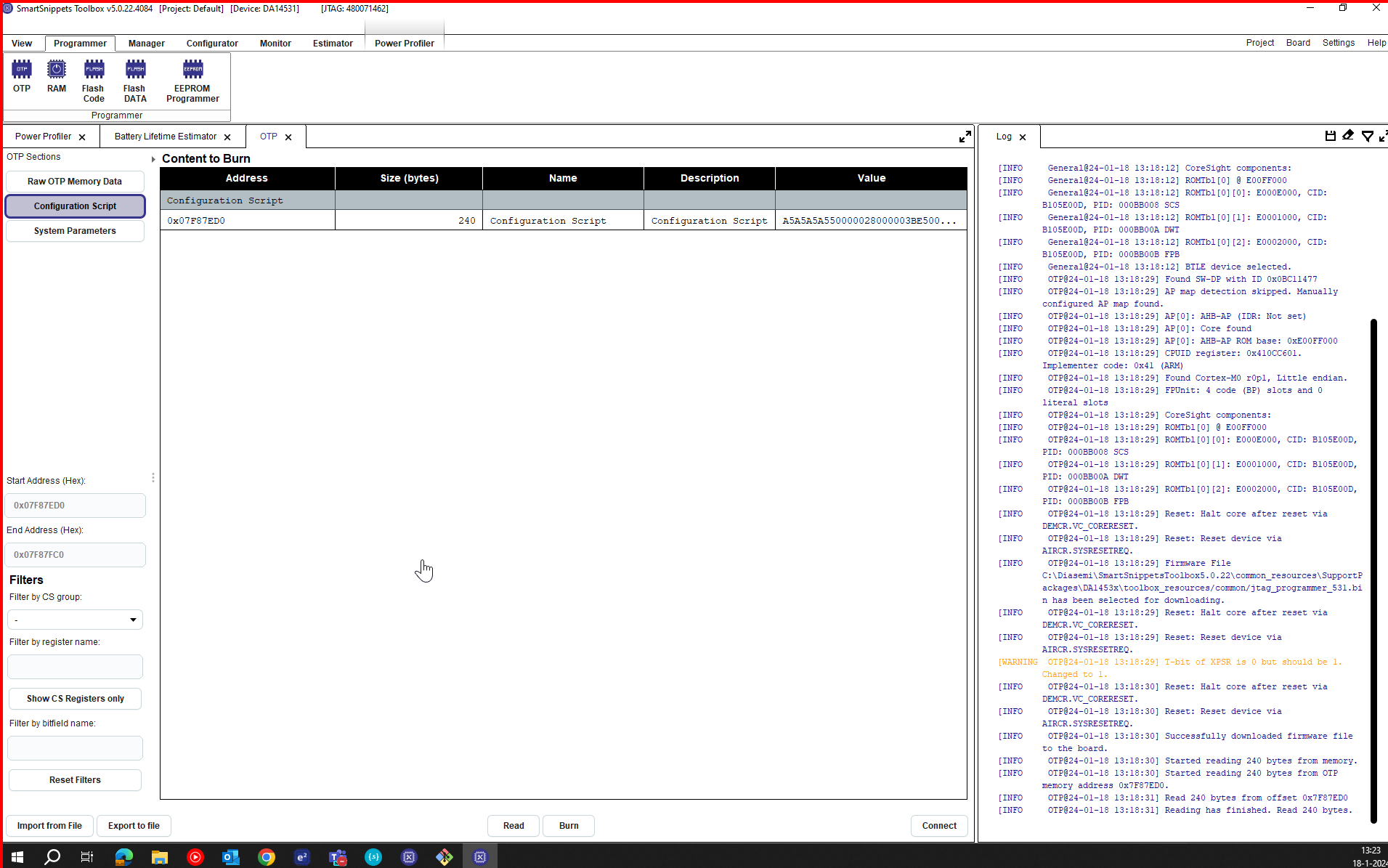
Figure 32 OTP tab
- To write on this register first on
- Click on the Configuration Script in the table. In the
Manage Configuration Scriptwindow you will see the following result: 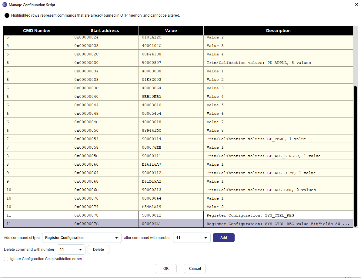
Figure 33 Configuration Script
- Click on the Configuration Script in the table. In the
- In
Add command of type, you will see a menu of different commands , chooseRegister Configurationand then click onADD 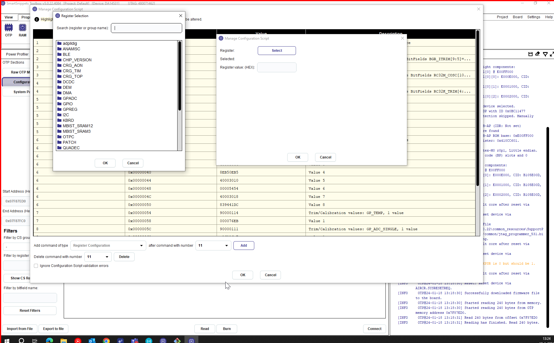
Figure 34 Register Selection
- In
- In
selectof register , typesys_CTRL_REG. Write the value1A1. 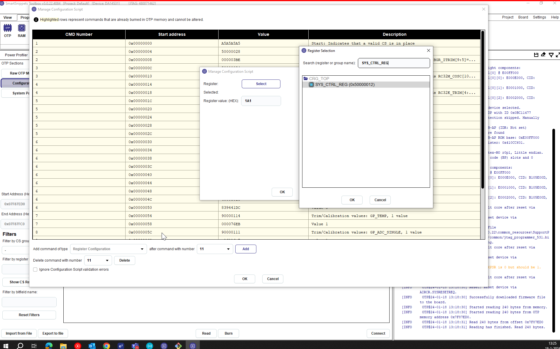
Figure 35 Select and write the HEX value
- In