5. DA1459x – The hardware
DA14592 DEVKIT-PRO and DA14594 DEVKIT-PRO
The DA14592 DEVKIT-PRO and DA14594 DEVKIT-PRO share the same motherboard. The only difference between these two development kits lies in their respective daughterboards. What applies to the DA14592 is equally applicable to the DA14594. For clarity, this section focuses on the hardware, using the DA14592 Dev Kit as an example.
The DA14592 DEVKIT-PRO consists of a main board DA14592-00HQDEVKT-P and a DA14592-00HQDB-P daughter board featuring the DA14592 SoC. More details about the DA1459x product family can be found in the DA1459x Datasheet.
5.1. The DEVKIT-PRO main board
Figure 1 illustrates the physical layout of the DEVKIT-PRO. The daughter board containing the DA1459x device is shown in Figure 3.
The DEVKIT-PRO main board provides all necessary hardware to enable:
Full functional verification of the DA1459x with the ability to take precise power measurements by isolating the DA1459x device.
Full digital connectivity with external hardware using UART, SPI and I2C.
USB-based debugging capabilities using the SEGGER J-Link on-board debugger for Cortex M33 processor.
USB-based UART communication with the host PC using a Future Technology Devices International (FTDI FT2232H) chipset which converts UART to USB.
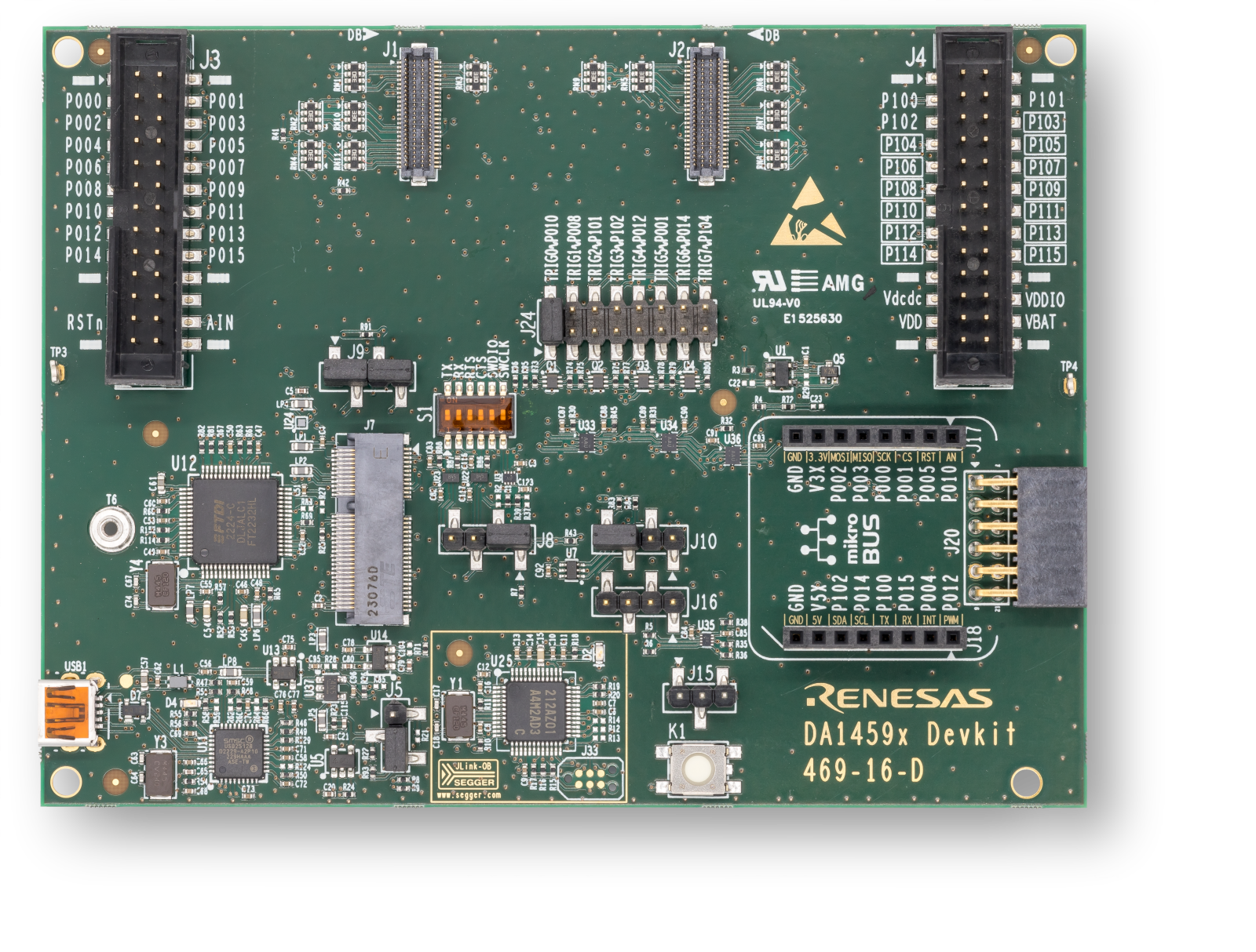
Figure 1 The DA1459x DEVKIT-PRO Motherboard
Note
J3 and J4 (Reference in Figure 1) are the Breakout Headers (2 pcs 2x13pin) for monitoring GPIO and power signals, with markings of signal names on the PCB top silkscreen.
Note
For current measurement using SmartSnippets Toolbox, you should power the main board by the USB connector.
5.2. The DEVKIT-PRO daughter board
The DEVKIT-PRO main board should be combined with the daughter board shown in Figure 2.
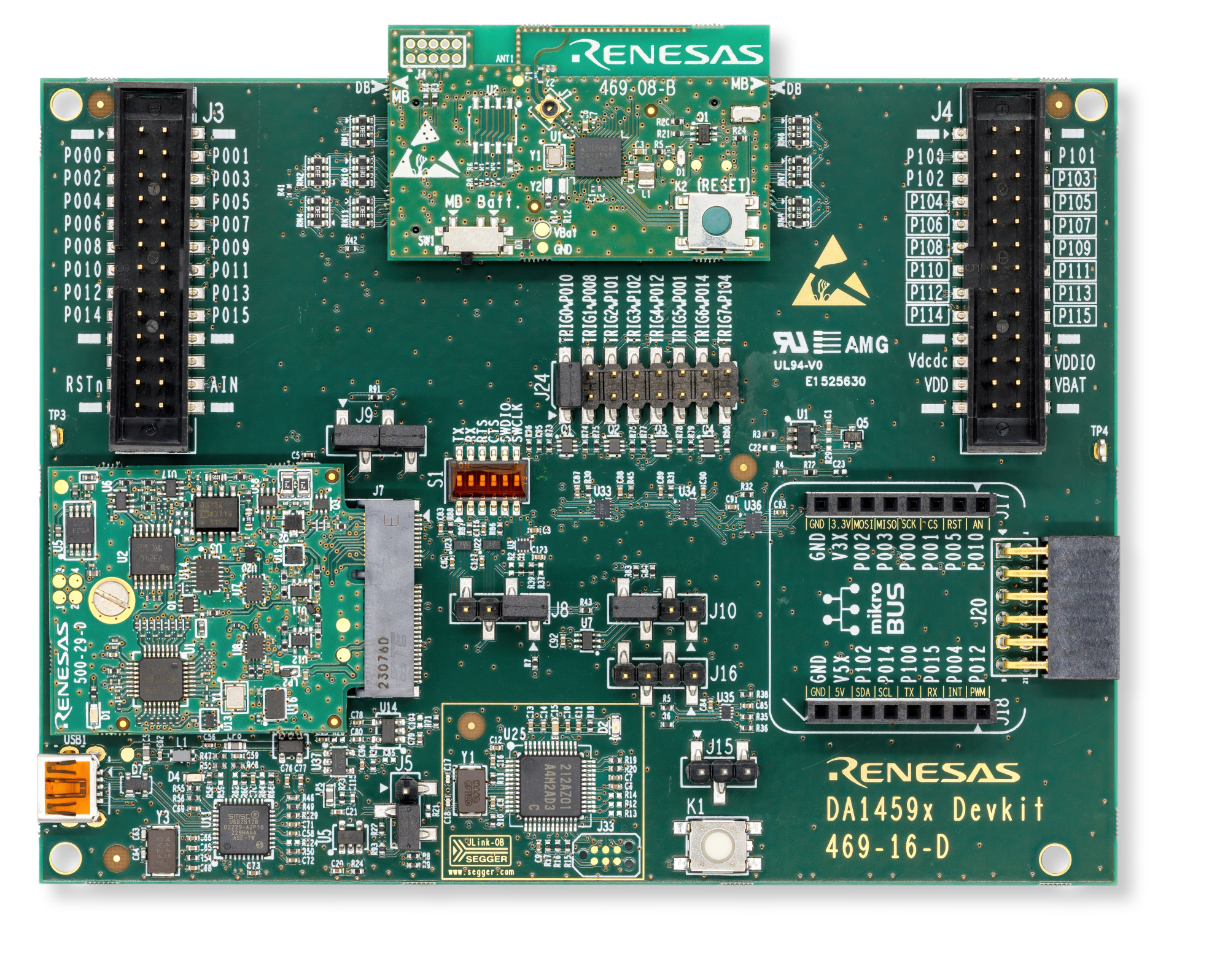
Figure 2 DA14592 DEVKIT-PRO
Figure 3 presents the DA14592 daughter board Layout and Figure 4 presents the DA14594 daughter board Layout.
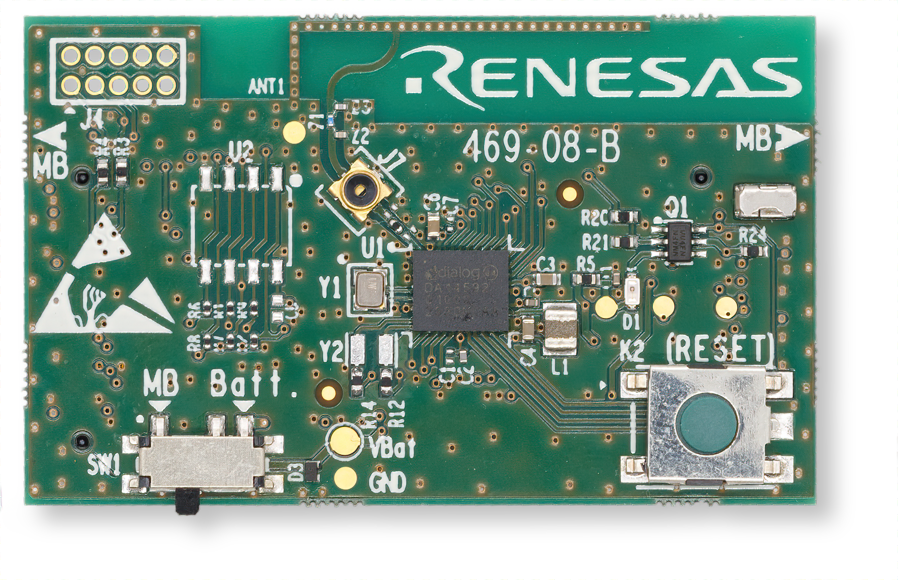
Figure 3 The DA14592 daughter board Layout
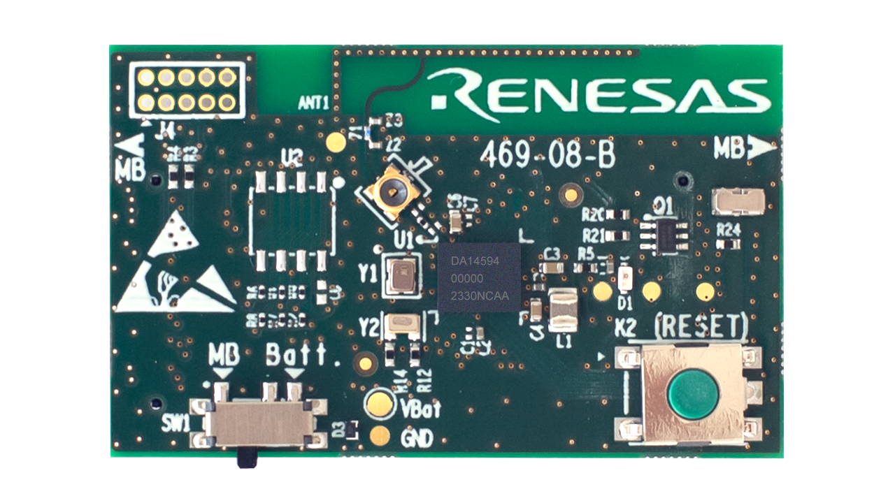
Figure 4 The DA14594 daughter board Layout
Note
The daughter board has a switch (referenced in Figure 3 or in Figure 4) to select the power source for the device. When the switch is in the left position, the daughterboard is powered by the motherboard (default) and when the switch is in the right position the daughterboard can be powered by a battery.
Note
The daughter board has the possibility to operate stand-alone (without the mother board), powered from one of these options:
Li-Ion/Coin Cell Battery (Max. 3.6V)
Main Development Board
Note
The schematic diagrams, BOM, and Gerber files are illustrated in detail in the DA14592 DEVKIT-PRO Documentation and DA14594 DEVKIT-PRO Documentation.
5.3. Connecting the DEVKIT-PRO to the host PC
The DEVKIT-PRO is connected to the host PC over the connector marked as USB1, as shown in Figure 1 using a standard mini-USB cable.
Note
Before connecting the DEVKIT-PRO Development Kit to the host PC make sure that :
The main board and the daughter board module are properly connected.
The switch on the daughter board is in the left position.
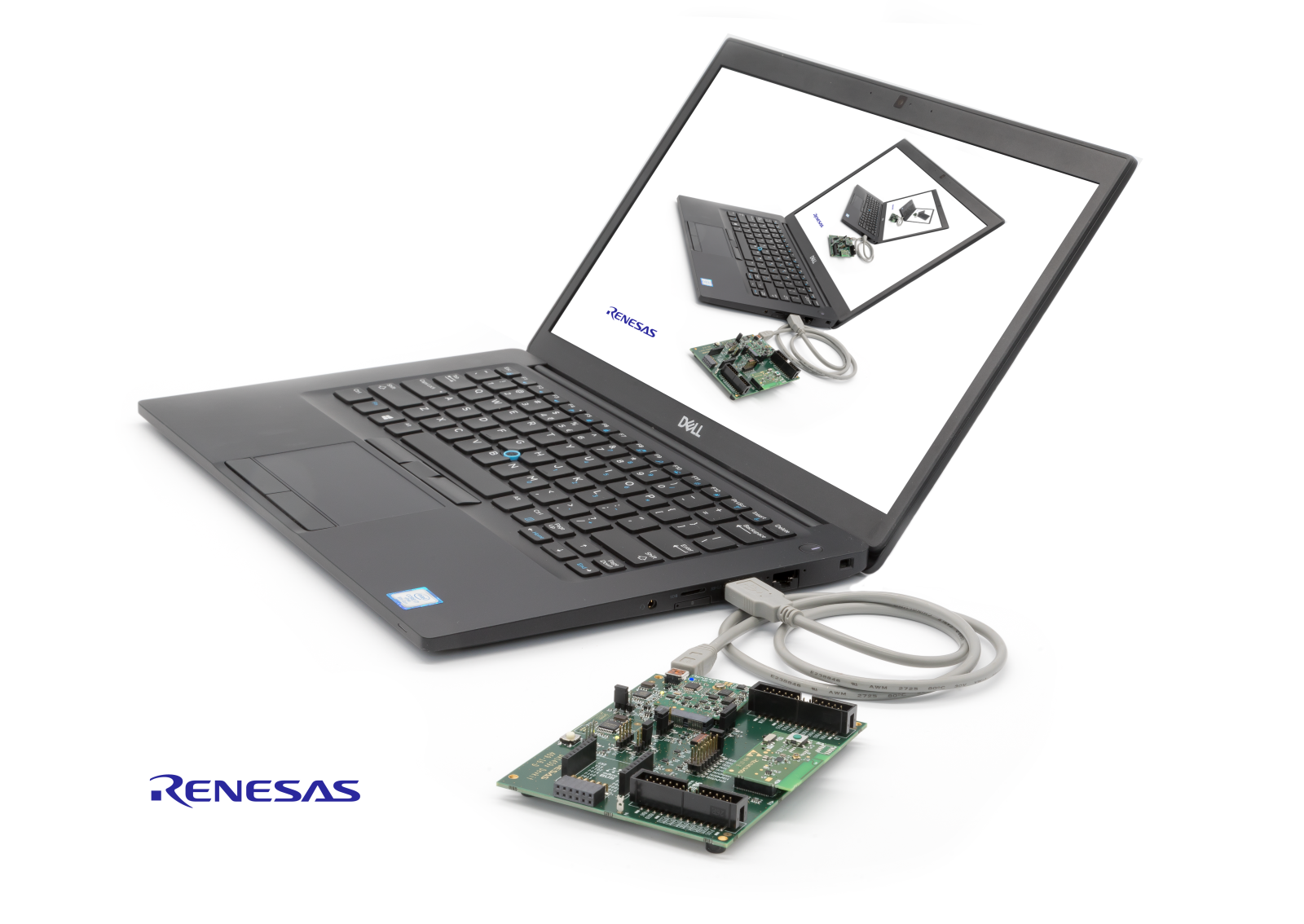
Figure 5 DEVKIT-PRO connections