5. DA1470x – The hardware
The Pro Development Kit (ProDK) consists of a main board (MB-PRO) DA1470x-00HQDEVKT-P and a DA1470x-00HQDB-P daughter board featuring DA14706 SoC of the desired package (VFBGA142). More details about the DA1470x products family is shown in Figure 1.

Figure 1 The DA1470x Product Family
5.1. The ProDK main board
Figure 2 illustrates the physical layout of the ProDK. The daughter board containing DA14706 device is shown in Figure 4.
The ProDK main board provides all necessary hardware to enable:
Full functional verification of the DA1470x family of products with the ability to take precise power measurements by isolating the DA14706 device.
Full digital connectivity with external hardware using UART, SPI and I2C.
USB based debugging capabilities using the SEGGER J-Link on-board debugger for Cortex M33 and Cortex M0+ SNC processor.
USB based UART communication with the host PC using a Future Technology Devices International (FTDI FT2232H) chipset which converts UART to USB.
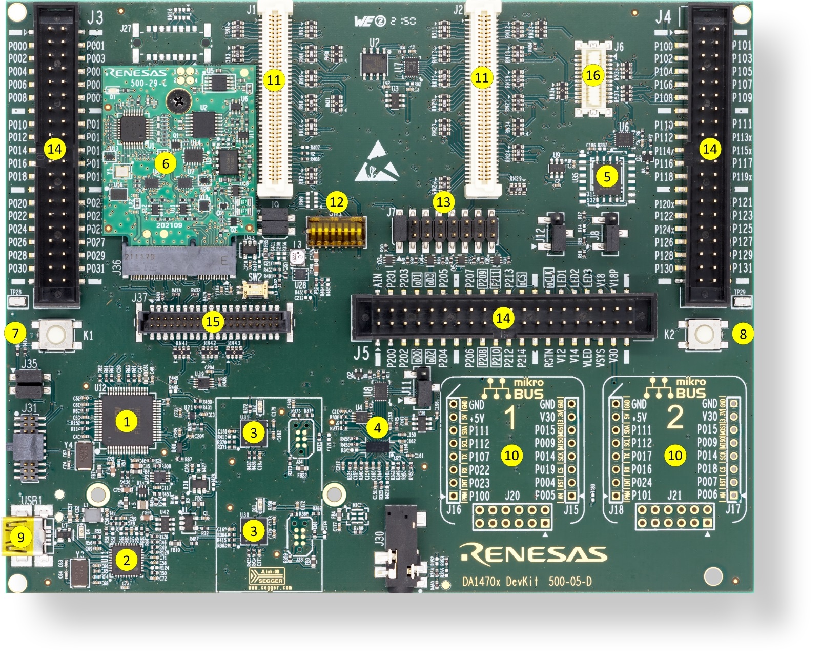
Figure 2 The DA1470x ProDK
Reference |
Description |
|---|---|
1 |
FTDI Chip |
2 |
USB HUB |
3 |
Segger Debug Interface |
4 |
Audio Codec |
5 |
Quad SPI Flash |
6 |
Power Measurement Circuit |
7 |
User button (K1) |
8 |
User button (K2) |
9 |
USB connector for power and communication interface |
10 |
mikroBUS™ sockets |
11 |
J1/J2 Daughter Board connectors |
12 |
DIP switch (SW1) Debugging Interface & UART |
13 |
Software Trigger Jumpers |
14 |
Signal/Power breakout headers (J3, J4, J5) |
15 |
LCD + CTP Connector |
16 |
eMMC DB Connector |
Note
J3, J4 and J5 (Reference 14 in Figure 2) are the Breakout Headers (3 pcs 2x20pin) for monitoring GPIO and power signals, with markings of signal names on the PCB top silkscreen.
Note
For current measurement circuit by SmartSnippets Toolbox (driven from a DA1470x GPIO, P0_16 ) you should power the main board by the USB connector.
5.2. The ProDK daughter board
The ProDK main board can be combined with the daughter board shown in Figure 4.
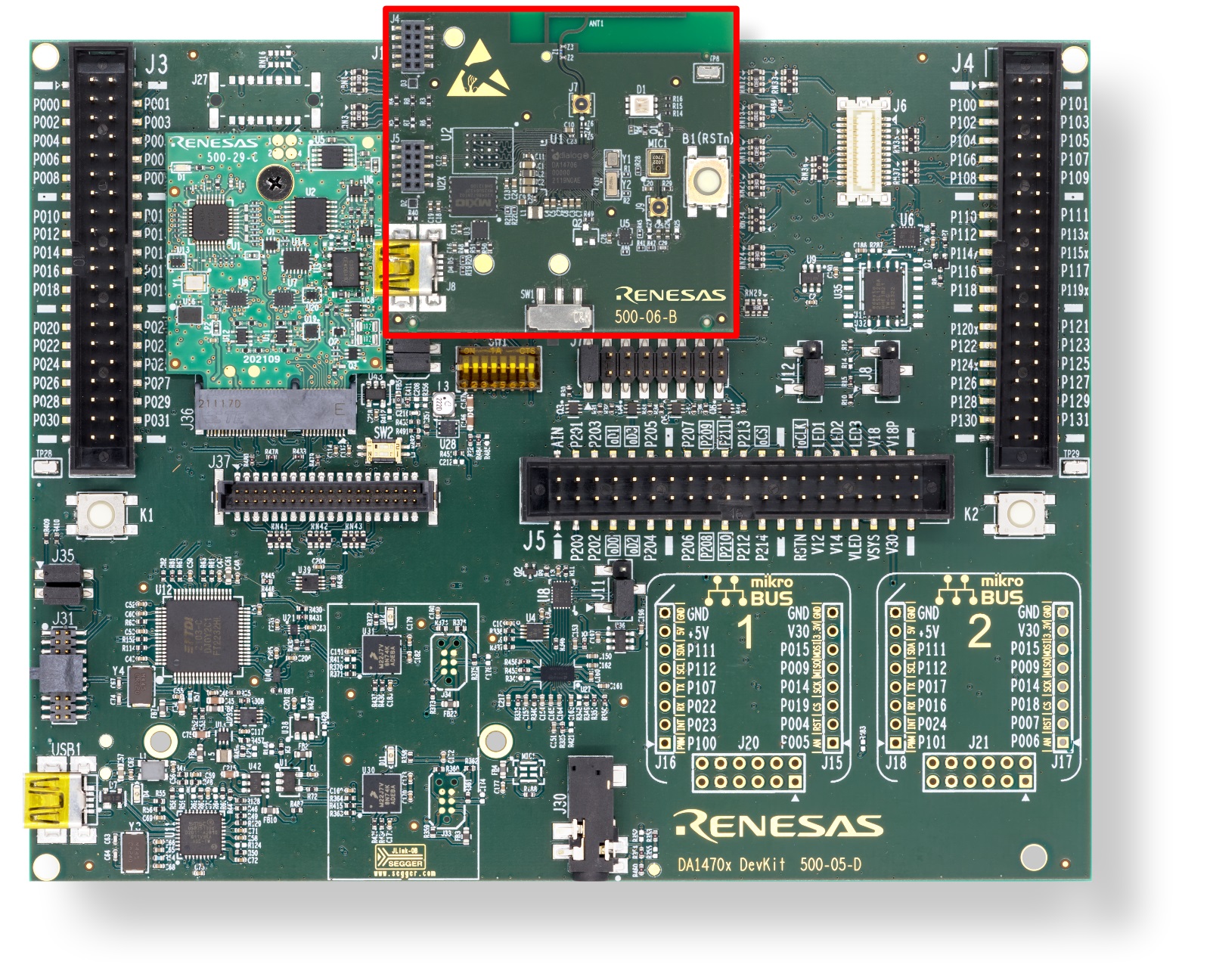
Figure 3 Main board - daughter board alignment
Figure 4 presents the DA14706 daughter board Layout.
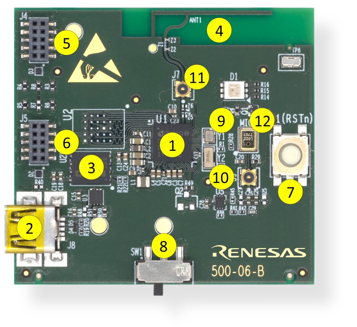
Figure 4 The DA14706 daughter board Layout
Reference |
Description |
|---|---|
1 |
DA14706 - BGA package |
2 |
USB power/charging |
3 |
OSPI/QSPI Flash |
4 |
Printed RF antenna |
5 |
M33 Debug Connector |
6 |
M0+ Debug Connector |
7 |
Reset |
8 |
Power Select |
9 |
Y1 : Crystal 32 Mhz |
10 |
Y2 : Crystal 32.768 KHz |
11 |
J7: Coaxial switch for conducted RF measurements |
12 |
Analog Microphone |
Note
The daughter board has a switch (reference 8 in Figure 4) to select the power supply for the device:
Power switch pos1 (left-default): VBAT LDO (default, this is the only option where the current is monitored by SmartBond™ Studio - Toolbox)
Power switch pos2 (right): Battery, Li-Ion (default) or Coin Cell
Note
The daughter board has the possibility to operate stand-alone (without the main board), powered from one of these options:
Li-Ion/LiPo/coin Battery
USB connector
5.3. The OLED display board
The ProDK main board can be combined with the OLED display board shown in Figure 5.
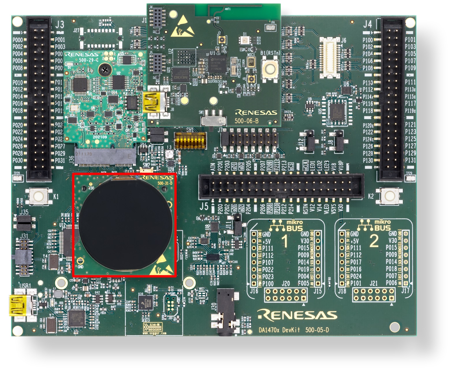
Figure 5 Main board - OLED display board alignment
Note
The schematic diagrams, BOM, and Gerber files are illustrated in detail in the Development Kit Documentation.
5.4. Connecting the ProDK to the host PC
The ProDK Development Kit allows functional verification of the DA1470x family of devices. It supports connecting external hardware by exporting DA14706 pins to standard headers and enables the user to do precise power measurements through the integrated power measurements circuitry.
The ProDev Kit motherboard also includes :
An embedded J-Link debugger
FTDI chip FT2232HL which allows easy communication with the development host over USB. The FT2232HL implements the USB to UART function and ensure the connectivity of the PC to the DA14706 SoC UART port and to current sense circuitry through SPI connection with ADC.
The ProDK Development Kit is connected to the host PC over the connector marked as USB1, as shown in reference 9 in Figure 2 using a standard mini-USB cable. For further reading you can refer to the Application Note: AN-B-087 DA1470x Application Hardware Design Guidelines and UM-B-148 The hardware of DA1470x Development kit
Note
Before connecting the ProDK Development Kit to the host PC make sure that :
The main board and the daughter board module are properly connected.
The power switch on the daughter board is in the left position.
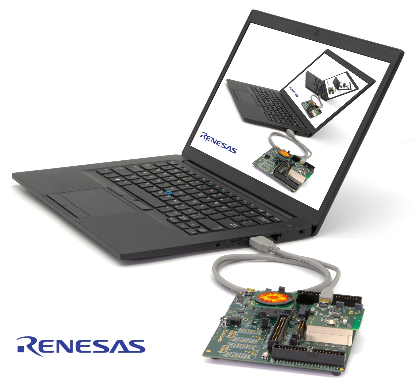
Figure 6 ProDK Development Kit connections