6. Introduction
As IoT devices evolve and become more sophisticated, LCD interfaces become more and more an integral part of these devices. LCDs designed for these systems follow a wide range of interfaces as well as color depths and resolutions. The DA1470x family of devices integrates an MCU capable to support all various combinations and signals with hardware acceleration, with an LCD controller capable of supporting the most commonly used interfaces (DBI-B, Dual SPI, Quad SPI, DPI-2, JDI Parallel, JDI SPI) and color depths. The LCD controller supports 2 HW layers with alpha blending, gamma correction LUT, dithering (Color Depth Degrading Method) and the base clock can reach up to 160MHz. Furthermore, there is a dedicated DMA engine used to fetch pixel data from the frame buffers and to transfer that data to the LCD controller, with image geometry and color format awareness. This means that the frame buffers (FBs) used to accommodate pixel data can be of any size and any supported color format, regardless of the actual output interface and color format.
Icons, graphs and animations are some of the most common ways to communicate events and data towards the end user of a product. Typically, these operations require some kind of data processing by invoking either a hardware accelerator or graphics library. The DA1470x family of devices supports graphics acceleration by using the D/AVE 2D GPU. For this application, the LVLG open-source lightweight library has been used, in order to achieve the desired high performance and sophisticated animations. For more information about the library, please refer to the official LVGL website.
In this context, the application’s structure is divided in 3 different areas, the application level, the SDK level, the HW level and finally the LCD Module where the graphical content is displayed. Figure 1 illustrates the application’s block diagram.
The UI Application consists of the screens, the icons, the animations and the actions/reactions triggered by the communicated events. The LVGL provides functions that handle common rendering tasks (some of them, hardware accelerated by the GPU). The GDI, which is an intermediate layer linking the Graphics Library with the LCDC adapter (including display-specific configuration file), and the I2C adapter used by the touch controller, is designed to provide an efficient, and display controller-independent graphical user interface for any application that operates with a graphical display.
The SDK consists of the GPU Driver providing an API to configure and control the GPU’s control registers, reading and writing the FBs. The LCDC Adapter is an abstraction layer placed on top of the LCDC LLD, providing multi-thread awareness and ensuring that the system remains awake for as long as the LCDC is in use and a drawing operation is in progress.
The HW level consists of the GPU, the Memory area and the LCDC. The GPU reads, processes, modifies and writes one of the available FBs - containing the pixel data, communicating with the memory area via a DMA channel. The Memory Area is divided in RAM, internal or external, and in FLASH cells. The internal System RAM is used to store the GPU commands list, the FBs and other operations (code, graphics library, additional resources). The external PSRAM is commonly used to store the FB when big display resolutions need to be supported. The external Flash memories can either be XIP, for storing code, textures (bitmap, icons, text), or background images, or Quad SPI NOR Flash for background image (Layer 0) or textures. Finally, the Display Controller (LCDC) blends each of the planes (FB, background image) into a single output image which is transferred to the LCD module.
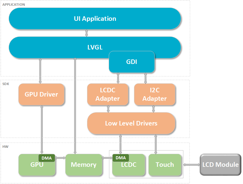
Figure 1 Block Diagram