5. Application Testing
5.1. Flow of the code
The protocol required to establish successful communication and to download the binary image into the DA1453x RAM is shown in Table 7 ‘Boot Protocol’ of AN-B-072.
As shown in Figure 49, the protocol starts with the DA1453x UART TX pin that transmits 0x02 (Start TX - STX). The Renesas microcontroller is expected to answer with a 0x01 (Start of Header - SOH) byte followed by 2 more bytes (LEN_LSB, LEN_MSB), which defines the length of the code to be downloaded (first byte is the least significant, second the most significant). The DA1453x answers with 0x06 (ACK) if the 3 bytes have been received and SOH has been identified, or answers with 0x15 (NACK) if anything went wrong. At this point the connection has been successfully established and the DA1453x image code code will start to be downloaded.
Upon completion of the required code bytes, the boot code calculates the CRC and send it over the URX. The boot sequence ends when the value 0x06 (ACK) is read at the URX line.

Figure 49 Flow of the code
5.2. GTL interface
GTL refers to the encapsulation of kernel messages for use with an External Processor. In its standard offering, GTL is supported over 4-wire UART. In the BLE SoC ROM, there is a dedicated kernel task (GTL Task) that is responsible to:
Decode the encapsulated kernel messages received from the External Processor and forward them to the respective BLE SoC tasks.
Encapsulate the kernel messages created by the various BLE SoC tasks and forward them to the External Processor over a wired h/w interface.
In the GTL architecture, a BLE application is running on the external host (RA MCU). The DA14531 accommodates the link layer, the host protocols and the profiles, and the RA MCU implements the application functionality. In general, the two components could communicate via GTL over a serial link which can be either UART or SPI.
REASONS TO CONSIDER TO USE GTL:
The main reason to consider the use of GTL is the complexity of the application and most importantly the memory footprint which can be too large for DA1453x.
There are many applications where the BLE SoC is not used as the main microcontroller. In these cases, GTL is a perfect fit. It allows the customer develop and maintain the s/w of the product in a concise way.
This configuration typically requires only limited code modifications on the DA1453x SDK. So, the BLE part of the customer’s application can be easily maintained with no or little support from Renesas.
The Host stack is running on the DA1453x.
Profiles/Services can be implemented either on the external MCU or on the DA1453x
GTL is straightforward to analyze and debug.
GTL can allow for drop-in replacement of the BLE SoC.
You can refer to the UM-B-143 Renesas External Processor Interface GTL for more details about Renesas GTL protocol.
Once the GTL binary image is loaded from Renesas MCU into DA1453x, the two chips can now communicate with each other over the Renesas GTL interface via a 4-wire UART (Tx, Rx, RTS, and CTS).
As shown in Figure 50 the DA14531 will send a GTL message stating it has booted successfully DEVICE_READY_IND. In response to this message, the Renesas microcontroller will send a message to configure the DA1453x GAPM_SET_DEV_CONFIG_CMD. This message contains settings like
device role, address, MTU. The DA1453x will respond to report whether configuration was successfull. After configuration, the DA1453x is ready to start advertising. A start advertising command GAPM_START_ADVERTISE_CMD
contains, among other things, advertising mode, advertising interval, advertising data and scan response data. After receiving this command, the DA1453x will start connectable advertising immediately.

Figure 50 GTL Interface
5.3. BLE profile validation
This section will walk you through validating your BLE profile. It shows how to use your smartphone to initiate a BLE connection. Ensure you have a BLE mobile application installed on your smartphone. For our purposes we will be using the Renesas Smartbond app.
Now you can use the Renesas Smartbond smartphone application to scan for the DA1453x BLE device.
Look for a device named what you selected in Figure 34. Click the blue arrow to the right to connect to the device and interrogate the GATT profile.
Here you will see the profile you set up earlier. Notice that the UUIDs that were generated previously are reflected here, your UUIDs will differ from what is in the image as they have been generated by the QE tool automatically.
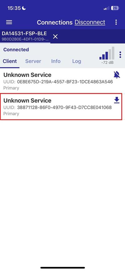
Figure 51 Renesas Smartbond application
Tap the characteristic that has the properties of Read and Write, remember that this characteristic was created to allow toggling of an LED.
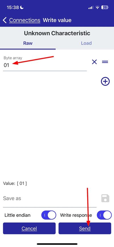
Figure 52 Renesas Smartbond Toggling Led
In the text box below the Write button type the value “01” and hit Send. This will send a new value to be written to the database on the chip. In turn our callback in
app_main.ctriggers, setting our LED. Verify that the Blue LED turns on with any value other than 0 and turns off on a 0.
5.4. What Next ?
This document doesn’t cover all the topics relevant to the DA1453x and FSP BLE Framework on Renesas Microcontrollers. It describes the first steps necessary to get started with the project. The following links provide more information:
DA14531 product web page To know more about the SmartBond™ DA14531 SoC.
Software example shows how Booting the DA14531 through a R7FA2E1 from RENESAS (EK-RA2E1). No GTL communication, just UART boot.
Renesas RA Family of 32-bit MCUs product page to learn about the four Renesas RA Family MCU series.