4. Middleware
4.1. System
4.1.1. Power and Clock Management
4.1.1.1. Introduction
This section illustrates :
The basic steps of the system when it goes to sleep and when it wakes up.
The supported power modes.
The basic system calls needed by the application to initialize the clock and the power management.
4.1.1.2. Going to sleep and waking up steps
The basic walk through is shown in Figure 4.
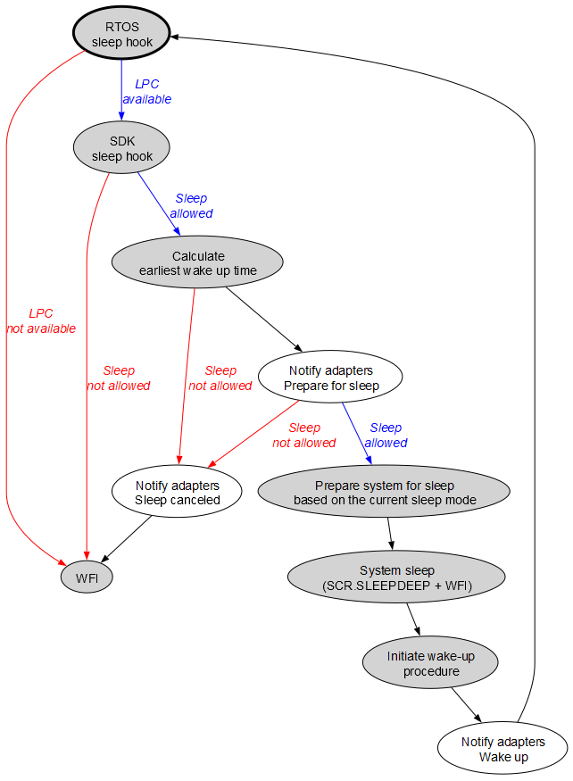
Figure 4 Going to sleep and waking up steps
Note
In case of different paths, the color of the arrow matches with the color of the comment.
4.1.1.3. Supported power modes
The supported power modes are depicted in Table 6.
Power mode |
Description |
|---|---|
active |
|
idle |
|
extended sleep |
|
deep sleep |
|
hibernation |
|
4.1.1.4. Initializing clock and power management
The flow for an application to initialize the clock and the power management is shown in Figure 5.
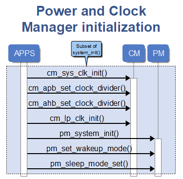
Figure 5 Power and clock manager initialization
4.1.2. Watchdog Service
The System Watchdog Service (sys_watchdog) has been designed to monitor
system tasks and avoid system freezes. The interaction of this service
with other parts of the system is shown in Figure 6:
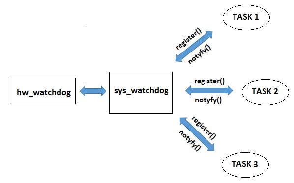
Figure 6 Watchdog overview
Effectively, sys_watchdog is a layer on top of the watchdog low-level driver
that allows multiple tasks to share the underlying hardware watchdog timer.
The service can be used to trigger a full system reset.
This will allow the system to recover from blocking situations in one or more tasks (infinite loops, resource locks etc.).
The hardware watchdog is essentially a countdown timer, which is powered by the always-on domain (PD_AON) and will be automatically enabled as soon as the system powers up. It is decremented by 1 every ~10 msec (RCLP) or ~21 msec (RCX) and it is set to a configured value at reset.
If WATCHDOG_CTRL_REG[NMI_RST] = 0, the watchdog timer will generate an
NMI to the Cortex M33 when the watchdog timer reaches 0 and a HW reset
when the counter becomes less or equal to -16. The NMI handler must write
any value > -16 to the WATCHDOG_REG to prevent the generation of a
watchdog reset within 16x10 = 160 ms. If WATCHDOG_CTRL_REG[NMI_RST] = 1, the
watchdog timer generates a reset if the timer becomes less than or equal
to 0. To prevent this, the watchdog timer can be reset to its starting value before
it expires.
If during one watchdog period all monitored tasks notify sys_watchdog,
the hardware watchdog will be updated; in this case, no platform reset will be triggered
for this watchdog period. A platform reset will be triggered if at least one task does not
notify sys_watchdog in time.
4.1.2.1. Registration - Notification scheme
A task that should be monitored has to first register itself with this service
to receive a unique handle (id). In case of any error during registration,
the invalid handle -1 is returned. After successful registration, a periodic
notification to sys_watchdog about the specific handle, signals that the
task is working properly.
There are two ways for a task to notify sys_watchdog.
Either the application is responsible for a periodic notification
from each registered task to the service before the watchdog expiration,
or a system-driven notification is sent by the sys_watchdog service towards the task.
In the latter case, a task must notify back after being notified by the system.
The notification scheme is defined per task upon registration with the service.
4.1.2.2. Suspend - Resume
Occasionally, the application may need to temporarily exclude a registered task from being monitored. This prevents a platform reset in cases where a task is expected to be blocked for a long time (ex. waiting for an event). There are available API functions to suspend and resume the monitoring of a specific task.
4.1.2.3. Latency skip
It may occur that a task needs a watchdog period greater than the configured
reset value. Calling a featured API allows a task to delay the
notification of sys_watchdog for a given number of watchdog periods,
without triggering a system reset. The effect of using the latency feature is
one-off, thus it must be set each time an increased watchdog period is required.
4.1.2.4. Configuration
The service is controlled in application level via the following configuration options in the custom header files.
Configuration macro |
Default value |
Description |
|---|---|---|
dg_configUSE_WDOG |
0 (disabled) |
Enable/Disable the watchdog service |
dg_configWDOG_MAX_TASKS_CNT |
8 |
Maximum number of tasks that the Watchdog Service can monitor |
dg_configWDOG_RESET_VALUE |
0xFF |
Reset value for Watchdog |
dg_configWDOG_IDLE_RESET_VALUE |
0x1FFF |
Reload value for watchdog when the system is idle (affects the sleep time) |
dg_configWDOG_NOTIFY_TRIGGER_TMO |
0 |
Watchdog interval to auto-notify registered tasks (msec) |
dg_configWDOG_GUARD_IDLE_TASK |
1 (enabled) |
Enable/Disable the idle-task registration with the watchdog service |
4.1.2.5. Examples
To register the task with sys_watchdog use the following code snippet
/* register an application task to be monitored by watchdog */
wdog_id = sys_watchdog_register(false);
To notify sys_watchdog use sys_watchdog_notify(). If the task execution flow is about to block (i.e. waiting for an event), then the task can be temporarily excluded from monitored with sys_watchdog_suspend(). As soon as the task is unblocked (i.e. event received) it can resume its watchdog operation with sys_watchdog_resume(). This flow is shown below :
/*
* notify watchdog on each loop since there's no other trigger for this - monitoring
* will be suspended while blocking on OS_TASK_NOTIFY_WAIT()
*/
sys_watchdog_notify(wdog_id);
/*
* Wait on any of the event group bits, then clear them all
*/
sys_watchdog_suspend(wdog_id);
ret = OS_TASK_NOTIFY_WAIT(0, OS_TASK_NOTIFY_ALL_BITS, ¬if, OS_TASK_NOTIFY_FOREVER);
/*
* Blocks forever waiting for the task notification. Therefore, the return value must
* always be OS_OK
*/
OS_ASSERT(ret == OS_OK);
sys_watchdog_resume(wdog_id);
4.1.3. API
Function |
Description |
|---|---|
int8_t sys_watchdog_register(bool notify_trigger) |
Register current task with the |
void sys_watchdog_unregister(int8_t id) |
Unregister task from the |
void sys_watchdog_suspend(int8_t id) |
Suspend task being monitoring by the A monitor-suspended task is not unregistered entirely, but it is ignored by the watchdog service until its monitoring is resumed. It is faster than unregistering and registering the task again. |
void sys_watchdog_resume(int8_t id) |
Resume monitoring of a task by the It should be called as soon as the reason that |
void sys_watchdog_notify_and_resume(int8_t id) |
Notify This function combines the functionality of |
void sys_watchdog_notify(int8_t id) |
Notify A registered task shall call this API function periodically to notify |
void sys_watchdog_set_latency(uint8_t id, uint8_t latency) |
Set watchdog latency for a task. This allows a task to miss a given number of notification periods to |
void sys_watchdog_idle_task_notify(void) |
Idle task should notify the When any other registered task notifies the service about its presence, the service assumes that the idle task is also alive. When no task has notified the service during dg_configWDOG_RESET_VALUE period, then it is expected that at least the idle task should be able to notify. In case this fails to happen, the platform is reset. |
4.1.4. ADC Service
4.1.4.1. Description
The system ADC service (sys_adc) has been designed to monitor periodically the on-chip temperature, detect a temperature
change, share temperature information with CMAC and start RCLP calibration when temperature exceeds specified limits. If RCX is used
as the system’s low power clock, then the service starts also the RCX calibration under certain temperature change. In addition,
the service triggers once a day the RC32M calibration.
The interaction of this service with other parts of the system is shown in Figure 7:

Figure 7 System ADC service overview
4.1.4.2. Concept
The sys_adc creates the Sys_ADC task and a periodic software OS timer sys_adc_timer. There are two possible events that will change the state of the Sys_ADC task from blocked to running, either a timer timeout or a trigger when system exits sleep. The latter will execute only if the time interval between the upcoming and last temperature measurement exceeds a specified time threshold. On both events, the task gets notified to measure and store the current temperature through the GPADC temperature channel, as well as to identify if the temperature delta from the previous measurement exceeds certain limits. In such a case, the rc_clocks_calibration_task is notified in order to execute the RCLP and the RCX calibration routines.
If the application requires BLE operations, the current temperature measurement is shared to CMAC. This is essential for CMAC and eventually the RF driver, in order to perform the RF calibration.
4.1.4.3. System use
The SmartSnippets™ DA1459X SDK enables and internally uses the service by default. Although it is not recommended, setting the dg_configUSE_SYS_ADC configuration option to 0 in the custom configuration header file (for example, custom_config_eflash.h) completely disables the service. Similarly, setting the dg_configRF_ENABLE_RECALIBRATION configuration option to 0 disables only the RF-calibration part of the ADC service, while the rest of the sys_adc functionality is not affected.
#define dg_configUSE_SYS_ADC (0)
#define dg_configRF_ENABLE_RECALIBRATION (0)
Note
The maximum timer period is defined internally by the SDK to 1sec. In case RF calibration is enabled (i.e. dg_configRF_ENABLE_RECALIBRATION
configuration option is set to 1) the timer period is the minimum between the time defined in dg_configRF_CALIB_TEMP_POLL_INTV configuration option and
the internally defined time of 1sec.
4.1.4.4. Audio Manager
4.1.4.4.1. Introduction
The Audio Manager is a middleware component for configuring the Audio Unit. It provides an API to setup and use the assorted audio paths available in this HW block.
4.1.4.4.2. Software architecture
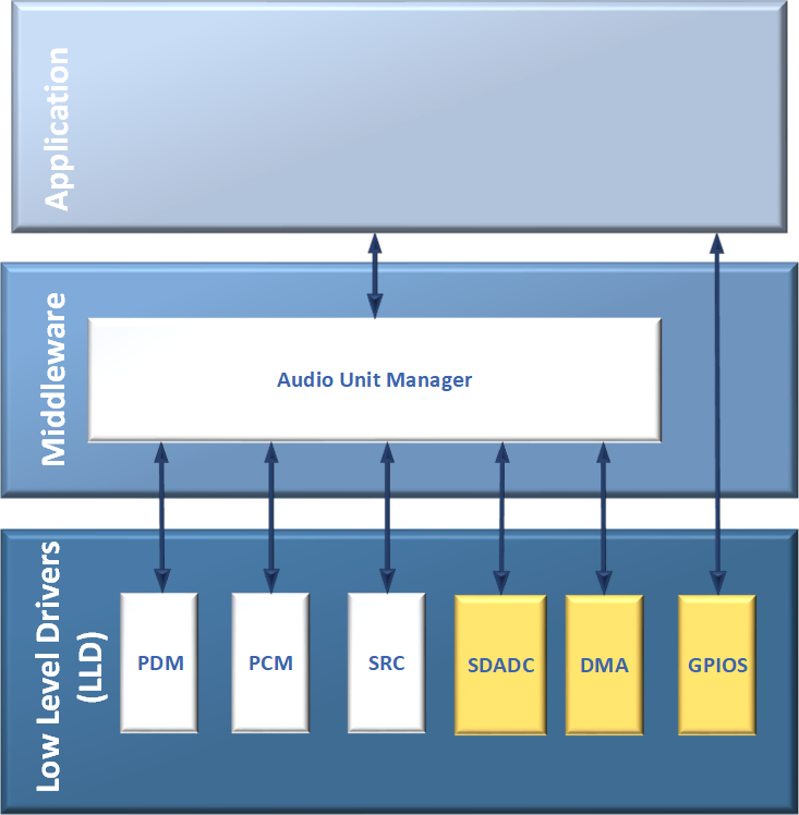
Figure 8 Audio Framework Architecture
As shown in the Audio Framework Architecture in Figure 8, the Audio Manager:
Provides an API for configuring, starting and stopping an audio path
Verifies that the requested audio path is supported
Interfaces with audio Low Level Drivers(LLD) and DMA
Does not configure GPIOS, this should be done by the application
Note: The yellow marked LLDs are not audio h/w blocks and need to be configured.
4.1.4.4.3. Audio Data Paths
The supported audio data paths are depicted in more detail in Figure 9.
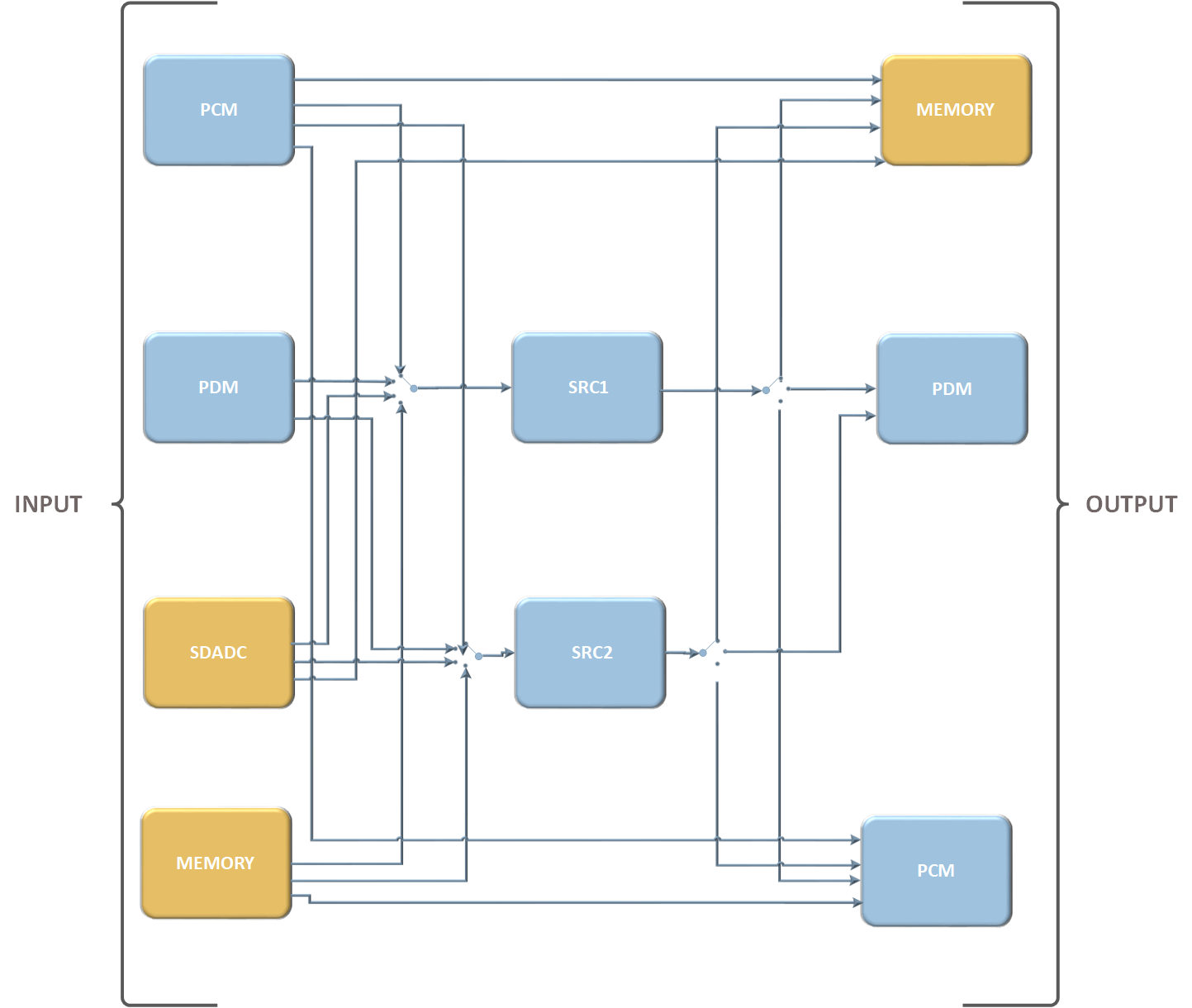
Figure 9 Audio Manager’s data paths
In DA1459x, up to 4 data paths are supported at the same time.
Examples:
Valid parallel paths:
Case 1
Input
SRCX
Output
MEMORY
No
PCM
SDADC
SRC1
PDM
PCM
No
MEMORY
MEMORY
SRC2
MEMORY
Case 2
Input
SRCX
Output
PCM
No
MEMORY
SDADC
No
MEMORY
PCM
SRC1
MEMORY
PDM
SRC2
MEMORY
The supported combinations of input and output interfaces for each data path are depicted in Table 9
Input |
SRCX |
Output |
|---|---|---|
PCM |
No |
PCM |
PCM |
Yes |
PDM |
PCM |
Yes |
MEMORY |
PCM |
No |
MEMORY |
PDM |
Yes |
PCM |
PDM |
Yes |
MEMORY |
MEMORY |
Yes |
PCM |
MEMORY |
No |
PCM |
MEMORY |
Yes |
PDM |
MEMORY |
Yes |
MEMORY |
SDADC |
Yes |
PCM |
SDADC |
Yes |
PDM |
SDADC |
Yes |
MEMORY |
SDADC |
No |
MEMORY |
The Audio Unit supports only one PCM interface, limited from the fact that both input and output PCM sample rates should be equal. Choosing a PCM audio path, the data is processed by handling the PCM’s own interrupts, rather than the SRC interrupt handling.
For data paths where memory is involved:
The DMA engine is used
If the input and output sample rates are equal, this renders the SRC engine obsolete, hence it is bypassed.
In data paths where memory is used as both input and output only sample rate conversions are applicable when the Audio Manager is used. A data path with memory as input and output, both having equal sample rates, is obsolete.
For data paths using SDADC the sole supported bit resolution is the one delivered by the SDADC filter, that being 16-bits.
In cases of simultaneous data path implementation, the supported parallel data paths follow the rules below:
PDM device may only be used once, either as input or as an output device for each data path, as PDM device has only one data pin that can be configured either as input or as output.
With the exception of MEMORY, each device-type can be used multiple times as input with all inputs sharing the same configuration and only once as output (if supported).
4.1.4.4.4. Configuring Audio Data Paths
In order to use the Audio Manager for configuring an audio path, the following steps are required:
Modify the application header file (for example,
custom_config_oqspi.h) as follows:#define dg_configSYS_AUDIO_MGR (1) #define dg_configUSE_HW_SRC (1)
In case PDM is used it must be added:
#define dg_configUSE_HW_PDM (1)In case PCM is used it must be added:
#define dg_configUSE_HW_PCM (1)In case SDADC is used it must be added:
#define dg_configUSE_HW_SDADC (1)Configure the interface pins (PCM, PDM):
PDM has the following configurable pins:
PDM_CLK_PIN : drives the clock signal
PDM_DATA_PIN : drives the input/output data signal
where x_x_PIN is defined as HW_GPIO_PORT_x GPIO_PIN_x
Pin configuration of PDM is depicted in Table 10
Mode |
Data Direction |
Pin configuration |
|---|---|---|
Master |
INPUT |
hw_gpio_configure_pin(PDM_CLK_PIN, HW_GPIO_MODE_OUTPUT, HW_GPIO_FUNC_PDM_CLK, false);
hw_gpio_configure_pin(PDM_DATA_PIN, HW_GPIO_MODE_INPUT, HW_GPIO_FUNC_PDM_DATA, false);
|
OUTPUT |
hw_gpio_configure_pin(PDM_CLK_PIN, HW_GPIO_MODE_OUTPUT, HW_GPIO_FUNC_PDM_CLK, false);
hw_gpio_configure_pin(PDM_DATA_PIN, HW_GPIO_MODE_OUTPUT, HW_GPIO_FUNC_PDM_DATA, false);
|
|
SLAVE |
INPUT |
hw_gpio_configure_pin(PDM_CLK_PIN, HW_GPIO_MODE_INPUT, HW_GPIO_FUNC_PDM_CLK, false);
hw_gpio_configure_pin(PDM_DATA_PIN, HW_GPIO_MODE_INPUT, HW_GPIO_FUNC_PDM_DATA, false);
|
OUTPUT |
hw_gpio_configure_pin(PDM_CLK_PIN, HW_GPIO_MODE_INPUT, HW_GPIO_FUNC_PDM_CLK, false);
hw_gpio_configure_pin(PDM_DATA_PIN, HW_GPIO_MODE_OUTPUT, HW_GPIO_FUNC_PDM_DATA, false);
|
PCM has the following configurable pins:
PCM_CLK_PIN : drives the clk signal
PCM_FSC_PIN : drives the FSC signal
PCM_DI_PIN : drives the input data
PCM_DO_PIN : drives the output data
where x_x_PIN is defined as HW_GPIO_PORT_x GPIO_PIN_x
Pin configuration of PCM is depicted in Table 11
Mode |
Data Direction |
Pin configuration |
|---|---|---|
MASTER |
INPUT |
hw_gpio_configure_pin(PCM_CLK_PIN, HW_GPIO_MODE_OUTPUT, HW_GPIO_FUNC_PCM_CLK, false);
hw_gpio_configure_pin(PCM_FSC_PIN, HW_GPIO_MODE_OUTPUT, HW_GPIO_FUNC_PCM_FSC, false);
hw_gpio_configure_pin(PCM_DI_PIN, HW_GPIO_MODE_INPUT, HW_GPIO_FUNC_PCM_DI, false);
|
OUTPUT |
hw_gpio_configure_pin(PCM_CLK_PIN, HW_GPIO_MODE_OUTPUT, HW_GPIO_FUNC_PCM_CLK, false);
hw_gpio_configure_pin(PCM_FSC_PIN, HW_GPIO_MODE_OUTPUT, HW_GPIO_FUNC_PCM_FSC, false);
hw_gpio_configure_pin(PCM_DO_PIN, HW_GPIO_MODE_OUTPUT, HW_GPIO_FUNC_PCM_DO, false);
|
|
SLAVE |
INPUT |
hw_gpio_configure_pin(PCM_CLK_PIN, HW_GPIO_MODE_INPUT, HW_GPIO_FUNC_PCM_CLK, false);
hw_gpio_configure_pin(PCM_FSC_PIN, HW_GPIO_MODE_INPUT, HW_GPIO_FUNC_PCM_FSC, false);
hw_gpio_configure_pin(PCM_DI_PIN, HW_GPIO_MODE_INPUT, HW_GPIO_FUNC_PCM_DI, false);
|
OUTPUT |
hw_gpio_configure_pin(PCM_CLK_PIN, HW_GPIO_MODE_INPUT, HW_GPIO_FUNC_PCM_CLK, false);
hw_gpio_configure_pin(PCM_FSC_PIN, HW_GPIO_MODE_INPUT, HW_GPIO_FUNC_PCM_FSC, false);
hw_gpio_configure_pin(PCM_DO_PIN, HW_GPIO_MODE_OUTPUT, HW_GPIO_FUNC_PCM_DO, false);
|
SDADC has the following configurable pins:
PGA_INP : drives the Programmable Gain Amplifier (PGA) positive input. This pin should be defined as HW_GPIO_PORT_1 GPIO_PIN_0, binding to the corresponding pin.
PGA_INM : drives the PGA negative input. This pin should be defined as HW_GPIO_PORT_1 GPIO_PIN_1, binding to the corresponding pin.
Pin configuration of SDADC is depicted in Table 12
Data Direction |
Pin configuration |
|---|---|
INPUT |
hw_gpio_configure_pin(PGA_INP, HW_GPIO_MODE_INPUT, HW_GPIO_FUNC_ADC, false);
hw_gpio_configure_pin(PGA_INM, HW_GPIO_MODE_INPUT, HW_GPIO_FUNC_ADC, false);
|
Initialize the HW resources (see examples below):
One Data Path: PDM to I2S
 #include "sys_audio_mgr.h"

 typedef struct {
         void *audio_dev;            //resource
         OS_TASK audio_task;
         sys_audio_path_t paths_cfg; // audio paths configurations
 } context_audio_demo_t;

 context_audio_demo_t context_audio_demo = {
     .audio_dev = 0,
     .audio_task = 0,
     .paths_cfg = {
             .audio_path[PATH_1] = {
                     .dev_in = (sys_audio_device_t*)&dev_1_in,
                     .dev_out = (sys_audio_device_t*)&dev_1_out,
             },
     },
 };

/* 1. Initialize parameters for PDM input */
 static  sys_audio_device_t dev_1_in = {
         /* Select interface as input of path 1 */
         .device_type = AUDIO_PDM,
         /* Initialize interfaces for input of path 1*/
         .pdm_param = {
                 .mode = MODE_MASTER,
                 .clk_frequency = 2000000, // Set PDM frequency in Hz
                 .in_delay = HW_PDM_DI_NO_DELAY,
                 .swap_channel = 0,
         },
 };

/* 2. Initialize parameters for I2S output */
 static sys_audio_device_t dev_1_out = {
         /* Select interface as output of path 1 */
         .device_type = AUDIO_PCM,
         /* Initialize interfaces for output of path 1*/
         .pcm_param = {
                 .bit_depth = 16, // Set I2S bit depth
                 .channel_delay = 0,
                 .clk_generation = HW_PCM_CLK_GEN_FRACTIONAL,
                 .clock = HW_PCM_CLK_DIVN,
                 .cycle_per_bit = HW_PCM_ONE_CYCLE_PER_BIT,
                 .format = I2S_MODE,
                 .fsc_delay = HW_PCM_FSC_STARTS_SYNCH_TO_MSB_BIT,
                 .fsc_length = 2,
                 .inverted_clk_polarity = HW_PCM_CLK_POLARITY_INVERTED,
                 .inverted_fsc_polarity = HW_PCM_FSC_POLARITY_NORMAL,
                 .mode = MODE_MASTER,
                 .output_mode = HW_PCM_DO_OUTPUT_PUSH_PULL,
                 .sample_rate = 16000, // Set I2S sample rate in Hz
                 .total_channel_num = 2,
         },
 };

 void audio_task()
 {
         /* 3. Open audio interfaces of audio for the required path */
         uint8_t idx_1 = sys_audio_mgr_open_path(dev_1_in, dev_1_out, SRC2); // Open path PDM to I2S

         /* 4. Enable resources of the required path. */
         sys_audio_mgr_start(idx_1); // idx_1 indicates return index of 'sys_audio_mgr_open_path'

         /* 5. Stop resources */
         sys_audio_mgr_stop(idx_1); // idx_1 indicates return index of 'sys_audio_mgr_open_path'

         /* 6. Close path */
         sys_audio_mgr_close_path(idx_1); // idx_1 indicates return index of 'sys_audio_mgr_open_path'
 }
- Two parallel Data Paths:
PDM to Memory
Memory to PCM
 #include "sys_audio_mgr.h"

 typedef struct {
         void *audio_dev;            //resource
         OS_TASK audio_task;
         sys_audio_path_t paths_cfg; // audio paths configurations
 } context_audio_demo_t;

 context_audio_demo_t context_audio_demo = {
     .audio_dev = 0,
     .paths_cfg = {
             .audio_path[PATH_1] = {
                     .dev_in = (sys_audio_device_t*)&dev_1_in,
                     .dev_out = (sys_audio_device_t*)&dev_1_out,
             },
             .audio_path[PATH_2] = {
                     .dev_in = (sys_audio_device_t*)&dev_2_in,
                     .dev_out = (sys_audio_device_t*)&dev_2_out,
             },
     },
 };

/* 1. Initialize parameters for PDM input */
 static  sys_audio_device_t dev_1_in = {
         .device_type = AUDIO_PDM,
         .pdm_param = {
                 .mode = MODE_MASTER,
                 .clk_frequency = 2000000, // Set PDM frequency in Hz
                 .in_delay = HW_PDM_DI_NO_DELAY,
                 .swap_channel = 0,
         },
 };

 /* 2. Initialize parameters for memory output */
 static sys_audio_device_t dev_1_out = {
         .device_type = AUDIO_MEMORY,
         .memory_param = {
                 .app_ud = 0,
                 .bit_depth = 16, // Set memory's bit depth
                 .buff_addr[0] = 0,
                 .buff_addr[1] = 0,
                 .cb_buffer_len = 1024,
                 .cb = audio_buffer_ready_cb_1,
                 .dma_channel[0] = HW_DMA_CHANNEL_0,
                 .dma_channel[1] = HW_DMA_CHANNEL_1,
                 .sample_rate = 8000, // Set memory's sample rate in Hz
                 .stereo = true,
                 .total_buffer_len = 1024 * 5,
                 .circular = false,
         },
 };

 /* 3. Initialize parameters for SDADC input of audio data path 2*/
 static sys_audio_device_t dev_2_in = {
         .device_type = AUDIO_MEMORY,
         .memory_param = {
                 .app_ud = 0,
                 .bit_depth = 16, // Set memory's bit depth
                 .buff_addr[0] = 0,
                 .buff_addr[1] = 0,
                 .cb_buffer_len = 1024,
                 .cb = audio_buffer_ready_cb_2,
                 .dma_channel[0] = HW_DMA_CHANNEL_2,
                 .dma_channel[1] = HW_DMA_CHANNEL_3,
                 .sample_rate = 8000, // Set memory's sample rate in Hz
                 .stereo = true,
                 .total_buffer_len = 1024 * 5,
                 .circular = false,
         },
 };

 /* 4. Initialize parameters for memory output of audio data path 2*/
 static sys_audio_device_t dev_2_out = {
         .device_type = AUDIO_PCM,
         .pcm_param = {
                 .bit_depth = 16, // Set I2S bit depth
                 .channel_delay = 0,
                 .clk_generation = HW_PCM_CLK_GEN_FRACTIONAL,
                 .clock = HW_PCM_CLK_DIVN,
                 .cycle_per_bit = HW_PCM_ONE_CYCLE_PER_BIT,
                 .format = I2S_MODE,
                 .fsc_delay = HW_PCM_FSC_STARTS_SYNCH_TO_MSB_BIT,
                 .fsc_length = 2,
                 .inverted_clk_polarity = HW_PCM_CLK_POLARITY_INVERTED,
                 .inverted_fsc_polarity = HW_PCM_FSC_POLARITY_NORMAL,
                 .mode = MODE_MASTER,
                 .output_mode = HW_PCM_DO_OUTPUT_PUSH_PULL,
                 .sample_rate = 16000, // Set I2S sample rate in Hz
                 .total_channel_num = 2,
         },
 };


 void audio_task()
 {
         for (uint8_t i = 0 ; i < (dev_1_out.memory_param.stereo ? 2 : 1); i++) {

                 if (dev_1_out.memory_param.dma_channel[i] != HW_DMA_CHANNEL_INVALID) {
                         if (size > OS_GET_FREE_HEAP_SIZE()) {
                                 dev_1_out.memory_param.buff_addr[i] = 0;
                                 return;
                         }
                         dev_1_out.memory_param.buff_addr[i] = (uint32_t)OS_MALLOC(size);

                         if (!dev_1_out.memory_param.buff_addr[i]) {
                                 ASSERT_ERROR(0);
                                 return;
                         }
                 }
         }

         for (uint8_t i = 0 ; i < (dev_2_out.memory_param.stereo ? 2 : 1); i++) {

                  if (dev_2_in.memory_param.dma_channel[i] != HW_DMA_CHANNEL_INVALID) {
                          if (size > OS_GET_FREE_HEAP_SIZE()) {
                                  dev_2_in.memory_param.buff_addr[i] = 0;
                                  return;
                          }
                          dev_2_in.memory_param.buff_addr[i] = (uint32_t)OS_MALLOC(size);

                          if (!dev_2_in.memory_param.buff_addr[i]) {
                                  ASSERT_ERROR(0);
                                  return;
                          }

                          demo_set_sinusoidal_pattern((uint32_t*)dev_2_in.memory_param.buff_addr[i],
                             dev_2_in.memory_param.total_buffer_len,
                             pcm_sin_data, ARRAY_LENGTH(pcm_sin_data),
                             dev_2_in.memory_param.sample_rate,
                             SIGNAL_INPUT_FREQ,
                             dev_2_in.memory_param.bit_depth);
                  }
          }
         /* 5. Open audio interfaces of audio for the required path */
         uint8_t idx_1 = sys_audio_mgr_open_path(dev_1_in,  dev_1_out, SRC1); // Open path 1 - PDM to Memory
         uint8_t idx_2 = sys_audio_mgr_open_path(dev_2_in,  dev_2_out, SRC2); // Open path 2 - Memory to PCM

         /* 6. Enable resources of the required paths. */
         sys_audio_mgr_start(idx_1); // idx_1 indicates return index of 'sys_audio_mgr_open_path' for path 1
         sys_audio_mgr_start(idx_2); // idx_2 indicates return index of 'sys_audio_mgr_open_path' for path 2

         /* 7. Stop resources */
         sys_audio_mgr_stop(idx_1); // idx_1 indicates return index of 'sys_audio_mgr_open_path' for path 1
         sys_audio_mgr_stop(idx_2); // idx_2 indicates return index of 'sys_audio_mgr_open_path' for path 2

         for (uint8_t i = 0 ; i < (dev_1_out.memory_param.stereo ? 2 : 1); i++) {
             if (dev_1_out.memory_param.buff_addr[i]) {
                         OS_FREE((void *)dev_1_out.memory_param.buff_addr[i]);
                 }
         }

         for (uint8_t i = 0 ; i < (dev_2_out.memory_param.stereo ? 2 : 1); i++) {
             if (dev_2_out.memory_param.buff_addr[i]) {
                         OS_FREE((void *)dev_2_out.memory_param.buff_addr[i]);
                 }
         }

         /* 8. Close paths */
         sys_audio_mgr_close_path(idx_1); // idx_1 indicates return index of 'sys_audio_mgr_open_path' for path 1
         sys_audio_mgr_close_path(idx_2); // idx_2 indicates return index of 'sys_audio_mgr_open_path' for path 2
 }
- Notes :
Set DIVN or DIV1 in application layer for PCM clock. Default value is DIVN.
- In case of employing memory as part of the data path, then there are limitations with respect to the size of the memory that can be allocated. These limitations derive from:
The total available heap memory size (
configTOTAL_HEAP_SIZE)The PCM sample rate or PDM frequency, PCM bit depth and the number of audio channels.
In case of using I2S, the number of channels must be 1 or 2 for one or two audio channels, respectively.
An example audio application is available in projects/dk_apps/demos/audio_demo folder.
4.1.5. Logging
In the SDK the supported method of logging is to use the standard C API printf() in the application code. There are four mutually exclusive configuration options that will override printf() in the file sdk/bsp/startup/config.c. These config options shall be set in the custom header files of your project, e.g config/custom_config_ram.h.
Warning
As printf() takes a variable length list of arguments and supports many formatting options the execution time and memory usage are unbounded. This can easily break an embedded system.
The recommendation is to be very careful with printf() .
Ideally use printf() in application tasks as they are lowest priority and tend to have larger stacks.
If it needs to log inside a high-priority RTOS task such as a timer callback then do not pass any variables to be parsed. Just print a short string with no formatting to avoid blowing the small 100 byte stack for the timer task and corrupting other variables.
Possible configuration options are as follows:
CONFIG_RETARGETIn this mode the logging data is redirected to a UART (ProDK and USB-Kit use UART2 by default) with an overridden version of the low level
API _write(). With this configuration theprintf()statements appear on the host PC on the lower numbered COM port that is enumerated for the USB cable (COMx for both Pro DK and USB-Kit on Windows,/dev/ttyUSB0for Pro DK and/dev/ttyACM0for USB-Kit on Linux).dg_configSYSTEMVIEWIn this mode the logging data is redirected to SEGGER’s SystemView tool running on the Host PC.
Note
SystemView only supports integer arguments, i.e. %d.
CONFIG_RTT
In this mode the logging data is redirected to a Segger Real Time Transfer (RTT) link which uses JTAG to communicate the data to the Segger RTT tools running on the Host PC.
Using RTT keeps the time taken for printf() to a minimum and allows printing debug information, while the application is performing time-critical, real-time tasks.
To view logging data in the host pc J-Link RTT Client Segger’s application shall be used.
To set and use RTT the follow steps must be done:
Get the RTT source files from the SEGGER J-Link software pack. You’ll mainly need:
SEGGER_RTT.c
SEGGER_RTT.h
Add RTT Files to Your Project
Copy SEGGER_RTT.c, SEGGER_RTT.h, and optionally SEGGER_RTT_printf.c to a folder in your project (e.g., src/segger_rtt/).
In e² studio:
Right-click your project → Properties → C/C++ General → Paths and Symbols
Under Includes, add the path to the RTT header files.
Initialize RTT in your Code
4.2. Adapters
4.2.1. Overview
The adapter scheme provides a transparent way for an application to access shared resources. The shared resources can be anything e.g data buffers, hardware resources etc see Figure 10. Hence, it can be considered as a thin layer which offloads the application from doing the resource management by its own.
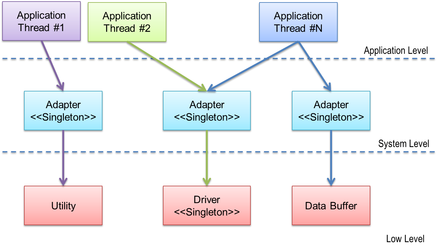
Figure 10 Adapter overview
The adapters use OS features such as semaphores, mutexes or events to synchronize resource-acquisition and resource-release requests. Their main goal is to provide a “thread-safe” access to the underlying shared resource see Figure 11.
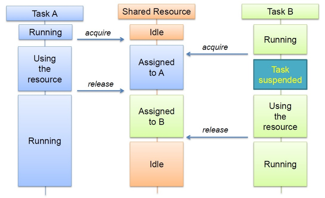
Figure 11 Adapter resource management
Note
It is recommended to access the harware resources via the adapter layer.
The adapter header files can be found under <SDK_ROOT_PATH>/sdk/middleware/adapters/include. Table 13
Filename |
Description |
|---|---|
ad_crypto.h |
ECC and AES/HASH device access API |
ad_flash.h |
Flash adapter API. |
ad_gpadc.h |
General Perpose Analog-Digital Converter adapter API. |
ad_i2c.h |
I2C device access API. |
ad_nvms.h |
adapter API. |
ad_nvms_direct.h |
Non-Volatile Memory Storage direct-access adapter API. |
ad_nvms_ves.h |
Non-Volatile Memory Virtual EEPROM Storage adapter API. |
ad_nvparam.h |
Non-Volatile Parameters adapter API. |
ad_nvparam_defs.h |
Non-Volatile Parameters adapter definitions. |
ad_pmu.h |
Power Manager adapter API. |
ad_sdadc.h |
Sigma Delta Analog-Digital Converter adapter API. |
ad_spi.h |
SPI adapter API. |
ad_template.h |
Template for a new adapter. |
ad_uart.h |
UART adapter API. |
4.2.2. Extending adapters for I/O-configured devices
Apart from the adapters essential to the system control (power management, non-volatile memory access, crypto device Access), the adapter concept has been extended for the following blocks:
All the serial interfaces (UART, I2C, SPI).
All the analog to digital converters GPADC or SDADC.
May the user implement a new adapter, the basic entities and relations of the adapter concept are explained in template source code in the adapter section.
Terminology |
Description |
|---|---|
Adapter |
A middleware abstraction layer for using a controller. It provides the following services:
|
Controller |
Top level view of a peripheral (e.g SPI, I2C), including the complete configuration needed for being fully functional (IOs, DMAs, Driver configuration) |
Driver (LLD) |
The Low Level Driver associated with the controller. |
Note
Depending on the peripheral there are configuration macros in low level drivers to enable or disable slave, DMA support or other features.
4.2.3. The UART adapter example
The UART adapter is an intermediate layer between the UART LLD and a user application. It allows the user to utilize the UART interface without implementing an Ad-Hoc resource management.
Features:
Provides a direction-specific resource management in order for the UART interface to be accessed in a “thread safe” manner by:
Different tasks.
Simultaneous read / write initiators.
Provides blocking and non-blocking read / write API.
Using the UART Adapter
Configure the UART adapter
To enable the UART adapter, the relevant macros need to enable the software controlling the UART interface. Configuration options affecting the UART interface define also the adapter’s behavior. These macros must be defined in the project’s custom header file, e.g
config/custom_config_ram.h.Table 15 uart config Configuration macro
Default value
Enable/Disable
dg_configUART_ADAPTER
0 (disabled)
UART adapter
dg_configUSE_HW_UART
1 (enabled)
UART driver
dg_configUART_DMA_SUPPORT
0
DMA support
dg_configUART_SOFTWARE_FIFO
0
Software FIFO support
dg_configUART_RX_CIRCULAR_DMA
0
DMA circular buffer for the RX channel
Create a UART controller configuration
ad_uart_controller_conf_t.
This is an example of a UART controller configuration taken from the file
sdk/middleware/adapters/src/sys_platform_devices_internal.c:
const ad_uart_io_conf_t sys_platform_console_io_conf = {
      /* Rx UART2 */
      .rx = {
            .port = SER1_RX_PORT,
            .pin = SER1_RX_PIN,
            /* On */
            {
                     .mode = SER1_RX_MODE,
                     .function = SER1_RX_FUNC,
                     .high = true,
            },
            /* Off */
            {
                     .mode = SER1_RX_MODE,
                     .function = SER1_RX_FUNC,
                     .high = true,
            },
      },
      /* Tx UART2 */
      .tx = {
            .port = SER1_TX_PORT,
            .pin = SER1_TX_PIN,
            /* On */
            {
                     .mode = SER1_TX_MODE,
                     .function = SER1_TX_FUNC,
                     .high = true,
            },
            /* Off */
            {
                     .mode = SER1_TX_MODE,
                     .function = SER1_TX_FUNC,
                     .high = true,
            },
      },
      /* RTSN */
      .rtsn = {
            .port = SER1_RTS_PORT,
            .pin = SER1_RTS_PIN,
            /* On */
            {
                     .mode = SER1_RTS_MODE,
                     .function = SER1_RTS_FUNC,
                     .high = true,
            },
            /* Off */
            {
                     .mode = SER1_RTS_MODE,
                     .function = SER1_RTS_FUNC,
                     .high = true,
            },
      },
      /* CTSN */
      .ctsn = {
            .port = SER1_CTS_PORT,
            .pin = SER1_CTS_PIN,
            /* On */
            {
                     .mode = SER1_CTS_MODE,
                     .function = SER1_CTS_FUNC,
                     .high = true,
            },
            /* Off */
            {
                     .mode = SER1_CTS_MODE,
                     .function = SER1_CTS_FUNC,
                     .high = true,
            },
      },
};
const ad_uart_driver_conf_t sys_platform_console_uart_driver_conf = {
     {

             .baud_rate = HW_UART_BAUDRATE_115200,
             .data = HW_UART_DATABITS_8,
             .parity = HW_UART_PARITY_NONE,
             .stop = HW_UART_STOPBITS_1,
             .auto_flow_control = 1,
             .use_fifo = 1,
             .use_dma = 1,
             .tx_dma_channel = HW_DMA_CHANNEL_3,
             .rx_dma_channel = HW_DMA_CHANNEL_2,
             .tx_fifo_tr_lvl = 0,
             .rx_fifo_tr_lvl = 0,
    }
 };

 const ad_uart_controller_conf_t sys_platform_console_controller_conf = {
     .id = SER1_UART, /* The UART interface dedicated to the platofrm */
     .io = &sys_platform_console_io_conf,
     .drv = &sys_platform_console_uart_driver_conf,
 };
User code
Initialize UART controller pins (optional)
The user is allowed to configure the I/O part of the controller before powering up the external connected devices (e.g sensors).
/**
 * \brief Initialize controller pins to on / off io configuration
 *
 * This function should be called for setting pins to the correct level before external
 * devices are powered up (e.g on system init). It does not need to be called before every
 * ad_uart_open() call.
 *
 * \param [in] id         controller instance
 * \param [in] io         controller io configuration
 * \param [in] state      on/off io configuration
 *
 * \return 0: success, <0: error code
 */
 int ad_uart_io_config (HW_UART_ID id, const ad_uart_io_conf_t *io, AD_IO_CONF_STATE state);
Note
The API function ad_xxx_io_config should be called after adapter’s mutex initialization from pm_system_init().
Open the UART controller
Before starting any read or write transaction the UART controller must be instantiated using Code 10.
/**
 * \brief Open UART controller
 *
 * This function:
 * - Acquires the resources needed for using the controller
 * - Configures the controller interface IOs
 * - Initializes the drivers associated with the controller
 *
 *
 * \param [in] ad_uart_ctrl_conf  controller configuration
 *
 * \return >0: handle that should be used in subsequent API calls, NULL: error
 *
 * \note The function will block until it acquires all controller resources
 */
ad_uart_handle_t ad_uart_open(const ad_uart_controller_conf_t *ad_uart_ctrl_conf);
Write/Read to/from the UART controller
Write and read API comes into two flavours, synchronous (blocking) and asynchronous (non-blocking):
Synchronous
Synchronous API suspends the calling task until the transaction is completed.
/**
 * \brief Perform a blocking write transaction
 *
 * This function performs a synchronous write only transaction
 *
 * \param [in] handle handle returned from  ad_uart_open()
 * \param [in] wbuf   buffer containing the data to be sent to the device
 * \param [in] wlen   size of data to be sent to the device
 *
 * \sa ad_uart_open()
 *
 * \return 0 on success, <0: error
 *
 */
int ad_uart_write(ad_uart_handle_t handle, const char *wbuf, size_t wlen);
/**
 * \brief Perform a blocking read transaction
 *
 * This function performs a synchronous read only transaction
 *
 * \param [in]  handle handle returned from ad_uart_open()
 * \param [out] rbuf   buffer for incoming data
 * \param [in]  rlen   number of bytes to read
 * \param [in]  timeout timeout time in ticks to wait for data
 *
 * \sa ad_uart_open()
 *
 * \note  If timeout is OS_EVENT_FOREVER, exactly \p rlen bytes must be received.
 *        If timeout is specified, function can exit after timeout with less bytes
 *        than requested.
 *
 * \return Number of transferred bytes on success, <0: error
 *
 */
int ad_uart_read(ad_uart_handle_t handle, char *rbuf, size_t rlen, OS_TICK_TIME timeout);
Asynchronous
Asynchronous API does not suspend the calling task. The task may continue with other operations. It will be notified via the registered callback function.
/**
 * \brief Perform a non blocking write transaction
 *
 * This function performs an asynchronous write only transaction
 * Caller task should retry until function returns no error
 * Callback will be called when transaction is completed
 *
 * \param [in] handle handle returned from ad_uart_open()
 * \param [in] wbuf   buffer containing the data to be sent to the device
 * \param [in] wlen   size of data to be sent to the device
 * \param [in] cb     callback to call after transaction is over (from ISR context)
 * \param [in] user_data user data passed to cb callback
 *
 * \sa ad_uart_open()
 *
 * \warning Do not call this function consecutively without guaranteeing that the previous
 *          async transaction has been completed.
 *
 * \warning After the callback is called, it is not guaranteed that the scheduler will give
 *          control to the task waiting for this transaction to complete. This is important to
 *          consider if more than one tasks are using this API.
 *
 * \return 0 on success, <0: error
 *
 */
int ad_uart_write_async(ad_uart_handle_t handle, const char *wbuf, size_t wlen,
                        ad_uart_user_cb cb, void *user_data);
/**
 * \brief Perform a non blocking read transaction
 *
 * This function performs an asynchronous read only transaction
 * Caller task should retry until function returns no error
 * Callback will be called when transaction is completed
 *
 * \param [in]  handle    handle returned from ad_uart_open()
 * \param [out] rbuf      buffer for incoming data
 * \param [in]  rlen      number of bytes to read
 * \param [in]  cb        callback to call after transaction is over (from ISR context)
 * \param [in]  user_data user data passed to cb callback
 *
 * \sa ad_uart_open()
 *
 * \warning Do not call this function consecutively without guaranteeing that the previous
 *          async transaction has been completed.
 *
 * \warning After the callback is called, it is not guaranteed that the scheduler will give
 *          control to the task waiting for this transaction to complete. This is important to
 *          consider if more than one tasks are using this API.
 *
 * \return 0 on success, <0: error
 *
 */
int ad_uart_read_async(ad_uart_handle_t handle, char *rbuf, size_t rlen, ad_uart_user_cb cb,
                       void *user_data);
See also
For more detailed information about how to enable asynchronous APIs please refer to Section 4.2.4.
Closing the UART device.
After completing the transactions and the UART controller instance is not needed anymore for additional tasks, it should be closed by using Code 15.
/**
 * \brief Close UART controller
 *
 * This function:
 * - Aborts ongoing transactions
 * - De-initializes the drivers associated with the controller
 * - Resets controller interface IOs (as specified in ad_uart_open())
 * - Releases the controller resources
 *
 * \param [in] handle handle returned from ad_uart_open()
 * \param [in] force force close even if controller is busy
 *
 * \sa ad_uart_open()
 *
 * \return 0: success, <0: error code
 */
int ad_uart_close(ad_uart_handle_t handle, bool force);
Example of a UART synchronous access:
static ad_uart_handle_t uart_handle;
static char wbuf[5] = "Test";
static char rbuf[5];

uart_handle = ad_uart_open(&ad_uart_controller_conf);                /* Open the UART controller */
ad_uart_write(uart_handle, wbuf, sizeof(wbuf));                      /* Write synchronously some data to UART controller */
ad_uart_read(uart_handle, rbuf, sizeof(rbuf), OS_EVENT_FOREVER);     /* Read synchronously the data from UART device */
ad_uart_close(uart_handle);                                          /* Close the UART controller */
4.2.4. Adapter’s configuration macros
This section describes available configuration macros in the adapter level
that enable or disable synchronous (blocking) and asynchronous (non-blocking)
API for read/write operations and resource locking.
YYY can be any of the serial interface, or ADC available adapters.
The macros are all enabled by default.
Enable synchronous transactions
The following macros are used in order to activate synchronous transactions, and can be found in each adapter’s header:
    /**
     * \def CONFIG_YYY_USE_SYNC_TRANSACTIONS
     *
     * \brief Controls whether YYY synchronous transaction API will be used
     *
     */
    #ifndef CONFIG_YYY_USE_SYNC_TRANSACTIONS
    #define CONFIG_YYY_USE_SYNC_TRANSACTIONS       (1)
    #endif
Enable asynchronous transactions
The following macros are used in order to activate asynchronous transactions, and can be found in each adapter’s header:
    /**
     * \def CONFIG_YYY_USE_SYNC_TRANSACTIONS
     *
     * \brief Controls whether YYY asynchronous transaction API will be used
     *
     */
    #ifndef CONFIG_YYY_USE_ASYNC_TRANSACTIONS
    #define CONFIG_YYY_USE_ASYNC_TRANSACTIONS      (1)
    #endif
Enable resource locking
The following macros are used in order to enable/disable resource locking. A simple scenario to use a peripheral via its adapter may allow to disable locking, producing a decreased size firmware.
/**
 * \def CONFIG_AD_YYY_LOCKING
 *
 * \brief Controls whether YYY adapter resource locking will be enabled
 *
 */
#ifndef CONFIG_AD_YYY_LOCKING
#define CONFIG_AD_YYY_LOCKING                     (1)
#endif
Warning
If resource locking is disabled, all such internal handling is disabled, thus becoming the application’s responsibility to handle concurrent accesses and controlling the resource management.
4.2.5. The NVMS Adapter
4.2.5.1. Introduction
This section provides information regarding the Non Volatile Memory Storage (NVMS) Adapter, which is responsible for accessing data from several memory resources. The NVMS Adapter is designed to simplify the tasks of reading, erasing, and writing non-volatile flash memories. It enables users to access both the Embedded flash memory (eFlash) of the device via Embedded Flash Controller (FCU), as well as any external QSPI flash memory (qFlash) connected to QSPI Controller (QSPIC), eliminating the need of dealing with low-level APIs.
4.2.5.2. Architecture overview
The software architecture for accessing the flash memories in SmartSnippets™ DA1459X SDK adopts a multi-layer approach depicted in Figure 12. At the topmost layer of this architecture resides the NVMS Adapter.
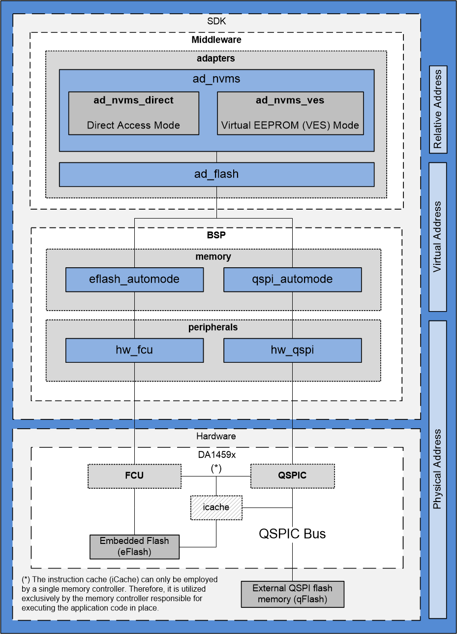
Figure 12 Architecture overview of NVMS Adapter
The architecture is composed of the layers presented in Table 16
Layer |
Description |
|---|---|
ad_nvms |
Thread safe API designed to handle NVMS partition. |
ad_flash |
Thread safe API designed to access the flash memories. |
eflash_automode/ qspi_automode |
APIs designed to access the eFlash and QSPI flash memories respectivelly. |
hw_fcu / hw_qspi |
Low level drivers responsible for handling the eFlash and QSPI controllers respectivelly. |
4.2.5.3. API Description
The APIs mentioned above utilize three types of addressing schemes: the relative, the virtual, and the physical address. The relative address refers to the data’s location in relation to the starting address of the partition, and its exclusively employed by the NVMS Adapter (ad_nvms) to offer a more user-friendly interface, eliminating the need for users to handle virtual or physical addresses directly. On the other hand, the flash memory controllers, FCU and QSPIC, rely on the physical address to access the data, which is solely used by the Low-Level Drivers, hw_fcu and hw_qspi.
4.2.5.4. Addressing schemes
The virtual address schema provides a unified address space, in which the accessible areas of all memory controllers are arranged consecutively, starting from 0x0. The Table 17 depicts the NVMS Virtual Address Map.
Memory controller |
Flash memory |
Virtual Base Address |
Virtual End Address |
|---|---|---|---|
FCU |
Embedded Flash memory. |
0x00000000 |
0x0003FFFF |
QSPIC |
External QSPI flash memory. |
0x00041000 |
0x02040FFF |
All API layers between the NVMS Adapter and the Low Level Drivers make use of the virtual address. This enables them to handle all flash memories as a unified memory space. The ad_nvms translates the Relative Address to Virtual Address, while the eflash/qspi_automode translates the Virtual Address to Physical Address (see Figure 12).
Addressing schemes |
API |
Description |
|---|---|---|
Relative address |
ad_nvms |
The address of the data with respect to the start address of a partition. |
Virtual address |
ad_flash, eflash_automode, qspi_automode |
The address of the unified memory space, where the accessible areas of the flash memories are placed one after the other staring from 0x00. |
Physical address |
hw_fcu, hw_qspi |
The physical address used by the flash memory controllers (eFlash, QSPIC) to access the data of the flash memories. |
4.2.5.5. Operation modes
The NVMS Adapter supports two operation modes, the Direct Access mode and the Virtual EEPROM mode.
Direct Access Mode
In Direct Access Mode, the data is written directly to the specified physical address. The API optimizes the flash memory access to minimize redundant erase and write cycles, in order to extend the memories lifespan following the next steps:
The API checks if the data in the destination address are the same as the data in the source address. If they are identical, both erase and write operations are skipped.
If the data in the destination address differ from the source data, the API checks if the source data can be written to the destination address without erasing the respective sectors, i.e. if no cleared bits in the destination address need to be set (0s to 1s). If this is the case, the erase operation is omitted. Otherwise, the erase operation becomes mandatory, and it is performed accordingly.
The source data are then written to the destination address.
It’s important to note that the Direct Access Mode does not provide protection against power failure. If a write operation requires a sector erase before writing, and a power failure occurs during this erase cycle, all data contained in this sector will be lost. For power-safe operations, the Virtual EEPROM Mode should be used.
Virtual EEPROM Mode
The Virtual EEPROM (VES) Mode utilizes a sophisticated approach to interact with flash memory aiming to extend its lifespan by implementing the following mechanisms:
Wear leveling
Wear leveling mechanism allows the flash memory to evenly distribute the write and erase cycles among all memory blocks. It prevents the premature wear-out of overused blocks, so all blocks can be used to the maximum. Wear leveling extends the life span and improves the reliability and durability of the storage device. However, it comes with the penalty that the available memory size becomes a fraction of the corresponding physical memory block.
This is accomplished by translating the user specified address into various physical addresses each time the contents of a particular location are modified. As a result, an additional virtual addressing mechanism comes into play, linking the user-provided address with a physical address that shifts with each data update. It’s important to differentiate this virtual addressing mechanism from the one mentioned in the Table 17, as it is solely relevant to the internal management of a VES partition.
The structure of a partition in VES mode is depicted in the Figure 13. Each partition is composed of multiple sectors, the number of which is determined by its size. In VES mode, flash sectors are subdivided into several containers, with each container storing data corresponding to a range of virtual EEPROM addresses. These containers include headers that retain their status (valid/dirty) and a 14-bit index, which serves to translate relative addresses into virtual addresses. Optionally, a CRC code field is also included. The Container Allocation Table (CAT) is responsible for mapping all data entries to their respective containers and sectors. During system startup, the CAT is initialized by extracting the necessary information from the indexes of the containers. It’s worth noting that smaller container sizes results to a higher number of erase cycles per sector.
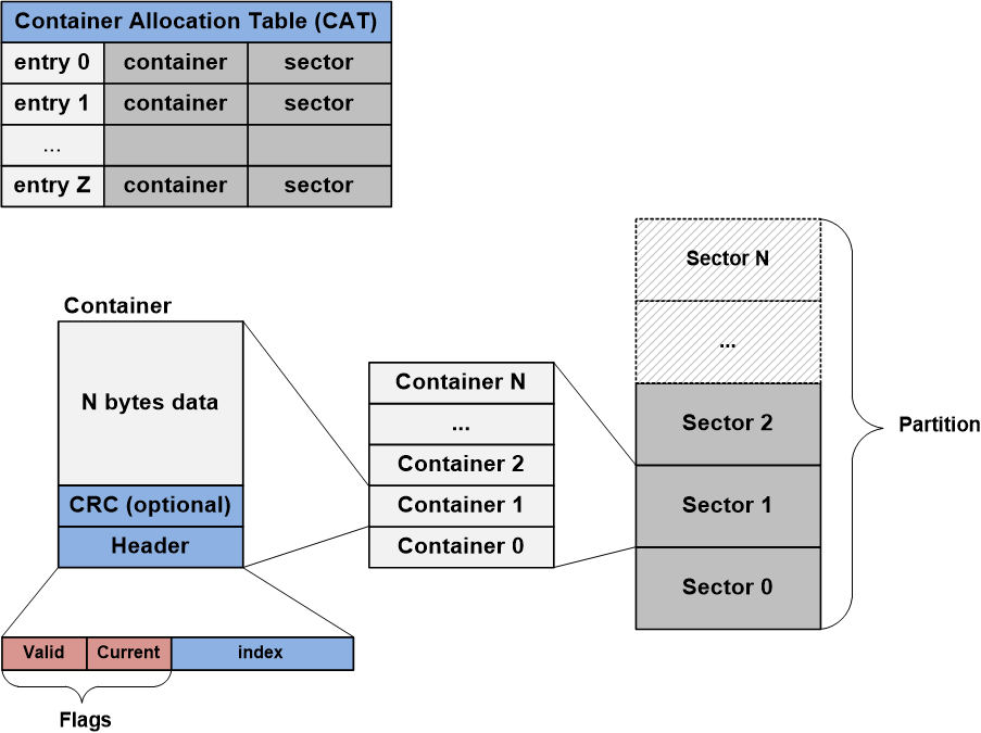
Figure 13 VES Storage Model DA1459X
Garbage Collection
Garbage collection is an additional technique for enhancing the operational lifespan and write efficiency of flash memory. Flash memory’s cells are organized into sectors, each encompassing multiple pages. While individual pages can be modified through write operations, a sector constitutes the minimum data block that can be erased using an erase operation. Consequently, updating a small number of bytes may lead to inefficient use of erase cycles for the unutilized pages within a sector.
More specifically, during wear leveling, when a new container is allocated, the old container is marked as dirty. As additional write operations are executed, the count of dirty containers rises, getting mixed with valid and free containers within the utilized sectors. Garbage collection is the process of consolidating valid containers and erasing sectors with only dirty containers. This is also called defragmentation. The garbage collector is executed when the amount of dirty containers within a sector exceeds a predefined threshold. Consequently, the valid containers are relocated to a new sector, and the existing sector is erased and marked as free.
Power failure protection
The VES Mode provides partition access that comes with protection against power failures. If a power failure takes place during a write operation, the specific data being written might be lost, while other data remains unaffected. This safeguard is achieved through the wear leveling mechanism outlined earlier.
4.2.5.6. Build Configuration
To activate the NVMS adapter both macros depicted in Code 20 must be set.
#define dg_configNVMS_ADAPTER         (1)
#define dg_configFLASH_ADAPTER        (1)
Additionaly, if at least one partition employs the Virtual EEPROM mode, it’s
imperative to set also dg_configNVMS_VES macro.
4.2.5.7. NVMS Partition Table
The Code 21 provides an example of an NVMS partition table designed for an application intended to execute from eFlash memory, with SUOTA support activated.
#define NVMS_PRODUCT_HEADER_PART_START  (EFLASH_MEM1_VIRTUAL_BASE_ADDR + 0x01000)
#define NVMS_PRODUCT_HEADER_PART_SIZE   (0x0001000)

#define NVMS_FW_EXEC_PART_START         (EFLASH_MEM1_VIRTUAL_BASE_ADDR + 0x02000)
#define NVMS_FW_EXEC_PART_SIZE          (0x001E000)

#define NVMS_FW_UPDATE_PART_START       (EFLASH_MEM1_VIRTUAL_BASE_ADDR + 0x20000)
#define NVMS_FW_UPDATE_PART_SIZE        (0x001E000)

#define NVMS_PARAM_PART_START           (EFLASH_MEM1_VIRTUAL_BASE_ADDR + 0x3E000)
#define NVMS_PARAM_PART_SIZE            (0x0001000)

#define NVMS_GENERIC_PART_START         (EFLASH_MEM1_VIRTUAL_BASE_ADDR + 0x3F000)
#define NVMS_GENERIC_PART_SIZE          (0x0000800)

#define NVMS_PARTITION_TABLE_START      (EFLASH_MEM1_VIRTUAL_BASE_ADDR + 0x3F800)
#define NVMS_PARTITION_TABLE_SIZE       (0x0000800)

PARTITION2( NVMS_PRODUCT_HEADER_PART  , 0 )
PARTITION2( NVMS_FW_EXEC_PART         , 0 )
PARTITION2( NVMS_FW_UPDATE_PART       , 0 )
PARTITION2( NVMS_PARAM_PART           , 0 )
PARTITION2( NVMS_GENERIC_PART         , PARTITION_FLAG_VES )
PARTITION2( NVMS_PARTITION_TABLE      , PARTITION_FLAG_READ_ONLY )
For every partition, it is necessary to create an instance of the macro PARTITION2(id, flags)
with a distinctive id and the corresponding flags. The id can be chosen from the enumerator
members detailed in Code 22, while the flags can adopt any
of the values listed in the Table 19.
/**
* \brief NVMS Partition IDs
*/
typedef enum {
NVMS_FIRMWARE_PART              = 1,
NVMS_PARAM_PART                 = 2,
NVMS_BIN_PART                   = 3,
NVMS_LOG_PART                   = 4,
NVMS_GENERIC_PART               = 5,
NVMS_PLATFORM_PARAMS_PART       = 15,
NVMS_PARTITION_TABLE            = 16,
NVMS_FW_EXEC_PART               = 17,
NVMS_FW_UPDATE_PART             = 18,
NVMS_PRODUCT_HEADER_PART        = 19,
NVMS_IMAGE_HEADER_PART          = 20,
} nvms_partition_id_t;
NVMS partition flags |
Description |
|---|---|
0 |
Direct mode partition with read/write access |
PARTITION_FLAG_READ_ONLY |
Direct mode partition with read only access |
PARTITION_FLAG_VES |
Virtual EEPROM mode partition |
In addition to the definition of PARTITION2(id, flags), it’s mandatory to also
define the macros id_START and id_SIZE which determine the virtual starting
address and the size of each partition, respectively.
4.2.5.8. API Description
The Table 20 lists the essential functions of the NVMS Adapter to access a flash memory:
NVMS Adapter essential functions |
Description |
|---|---|
ad_nvms_init() |
Initialize NVMS adapter |
ad_nvms_open() |
Open partition to perform a read/write access |
ad_nvms_read() |
Reads data from a specified partition |
ad_nvms_write() |
Writes data to a specified partition |
ad_nvms_erase_region() |
Erases a specified partition region |
The ad_nvms_init() is invoked during application startup to carry out all essential
initialization tasks, including the identification of the underlying memory partitions.
Actually, this function is called by pm_system_init(), which takes care of system
initialization after a power cycle. Prior to accessing a partition, the ad_nvms_open()
must be called to obtain its handler. Subsequently, the ad_nvms_read(), ad_nvms_write()
and ad_nvms_erase_region() are utilized to perform read, write and erase operations
respectively. As previously mentioned, the NVMS adapter operates on a relative addressing
scheme. Consequently, the aforementioned functions are limited to access a single partition.
If access to another partition is required, the same sequence must be repeated. The
Code 23 presents a typical example of employing the NVMS Adapter.
nvms_t partition = ad_nvms_open(NVMS_GENERIC_PART);

for (;;) {

   ad_nvms_read(partition, addr, buf, sizeof(buf));
   ad_nvms_write(partition, addr, buf, sizeof(buf));
}