6. Memory setup
6.1. System RAM Architecture
Focusing on CPUs, since all of them can have access to system RAM at the same time, in order to reduce multiplexing and timing constraints as much as possible, each CPU has access to a specific memory space range. In Figure 1, an overview is presented of the RAM setup, including the areas and corresponding address ranges that can be accessed by each CPU.
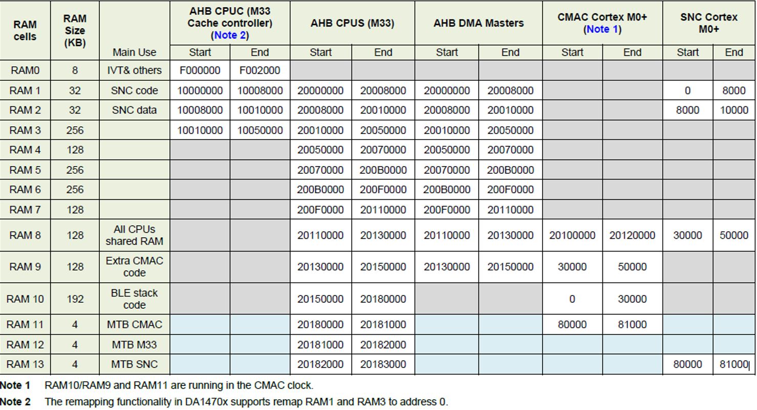
Figure 1 Memory Access by Each System Master
The grey area declares that the CPUs have no access to the specific RAM cell. The last three RAM cells, RAM11, RAM12 and RAM13, constitute the Micro Trace Buffer (MTB) area of each processor. SysCPU has access to all MTBs, while the other two CPUs can access only their own MTB area. RAM8 cell is used as common RAM space for inter-processor communication. The two memory cells, RAM9 and RAM10, which are used for CMAC code and data, belong to the CMAC clock domain (maximum frequency of 32 MHz). The access to these cells from the SysCPU is through an H2H bridge with wait states, due to clock domain crossing. For the same reason, the shared memory cell, RAM8, is accessed by CMAC through an H2H bridge with additional wait states.
6.2. System RAM Access
All CPUs support a “Ready” like signal functionality, so that they can be stalled for a specific amount of clock cycles. This makes the arbitration signals for the AHB interfaces (SysCPU, Display Controller, GPU, and General-Purpose DMA) HREADY, while the memory interfaces (MTB) should also support a respective input (MREADY) and should only proceed in reading/writing the RAM cell if this signal is high. The CMAC CMI interface does not support any MREADY functionality, so it always has the highest priority. An overview of the basic metrics of each master accessing the memory controller is shown in Figure 2.
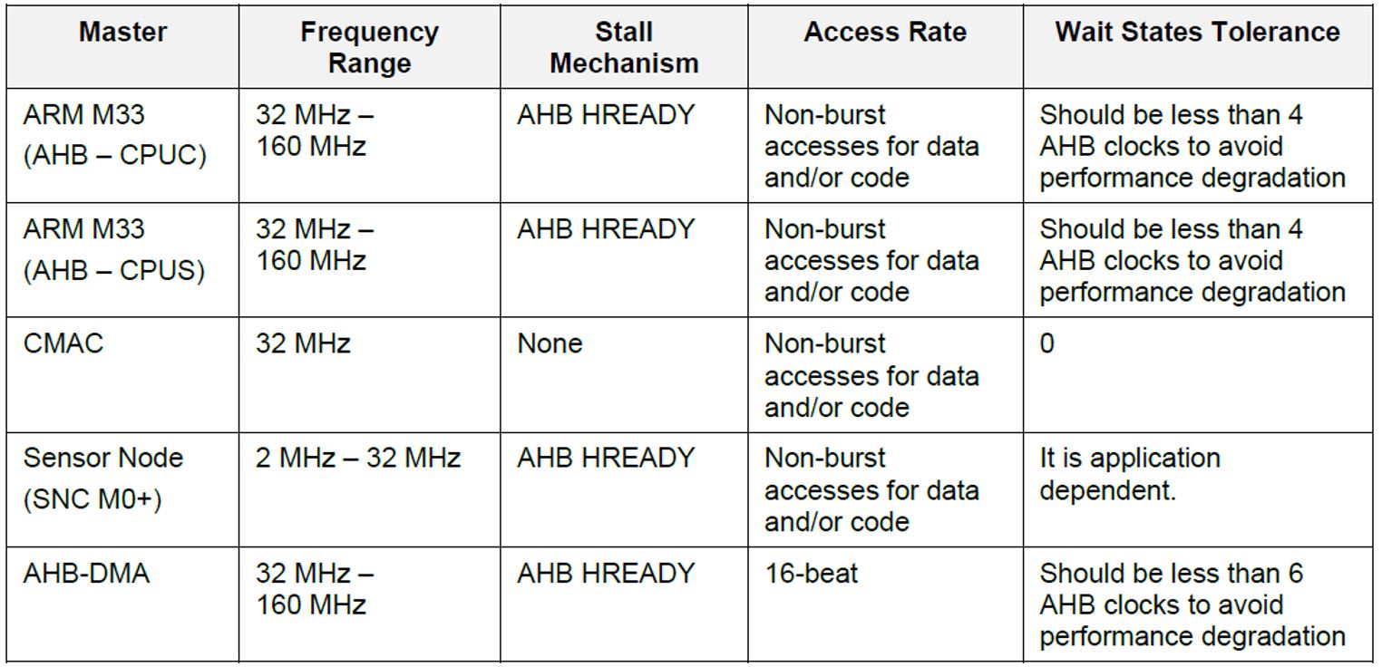
Figure 2 Memory Controller Masters Access Metrics
The arbitration scheme is round robin, which respects the wait states tolerance of each master. The maximum wait states tolerance for each master is programmable through the memory controller register file. Furthermore, the priorities of the masters for each of the eight arbitration engines (RAM1 to RAM8) are also programmable by SW. Finally, according to the system’s remapping functionality, RAM1 or RAM3 cells can be remapped to 0 by SW.