7. Your First Application
This section describes how to construct, create, and run a straightforward software application using the instructions for DEVKT-P users. Two examples for DA14535 are provided in this chapter, one to test the output and show how it functions and the other to use the BLE functionality. Step-by-step instructions are provided for loading the example as a project in the Keil® environment, setting up and building the project, and then executing the project using the debug environment on the DA14535 devices.
Security in SDK6 Examples
The various projects in the Renesas SDK come with the BLE security disabled by default. During the development phase of a project, this helps debugging a custom application and making a wireless connection to the device. For a production version, Renesas is strongly advising to enable the security settings on the available BLE services. DA145xx Tutorial BLE Security and the SDK6 example project ble_app_security explain on how the different security levels can be applied.
Make sure that you have all required tools installed as described in Section 5 and Section 6. The DA14535 Software Development Kit (SDK) includes examples that run on the DEVKT-P. The examples are provided with preconfigured Keil® projects.
Build Options
DA14535 and DA14531 software examples are included in the same SDK. This can be selected using the correct target option as indicated in Figure 24. For more information, see the DA1453x DA14585/586 Software Platform Reference (UM-B-119).
7.1. The Blinky Peripheral Example Application
Blinky is a simple application that demonstrates the basic initialization of DA14535 and LED blinking. This is a good example to test the hardware, connection to PC and making sure the SDK is downloading correctly.
After the SDK is downloaded, the blinky source code example is in the directory called peripheral_examples.
The figure below shows the procedure of building the source code example for DA14535.
The same process is applicable for the other chips in these families (DA1453x and DA1458x).
2-Wire UART Configuration for Blinky Project
- Table and figure below show the configuration for the 2-wire UART while only need Tx wire.
Table 6 Blinky example UART and LED jumper configuration for DA14535 GPIO
Function
Jumper
P0_6
UART2 TX (2 Wires)
Connect J1.17 - J2.27
P0_9
LED
Connect J8.3 – J8.4

Figure 21 UART2 2-wire jumper configuration DA143x DEVKIT-P
Single Wire UART
It is also possible to use single wire UART for this project. For more information about the configuration, see Appendices.
Open the folder that has the SDK files. Figure 22 shows the folder with the extracted SDK zip file.
In
<sdk_root_directory>\projects\target_apps\peripheral_examples\blinky\Keil_5, double-clickblinky.uvprojxto open the project in Keil®.
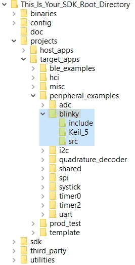
Figure 22 Blinky project directory
The development environment should look like the following figure when the project is opened with Keil®:
SDK6 Default Settings
These are the default settings on the latest SDK6 release. You do not need to make any change in the settings in this tutorial.
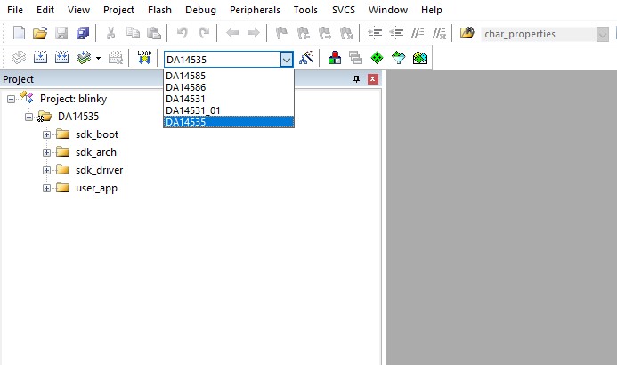
Figure 24 Blinky project Keil® workspace for DA14535
Click the Target Options button, and then select the Device tab. The dialog window should look like Figure 25.

Figure 25 Blinky project options
Click the Linker tab. Scatter files (
.sct) are used to select memory areas.

Figure 26 Blinky project scatter file
Click the Debug tab. Make sure that J-LINK/J-TRACE Cortex is selected and the Initialization File is correctly set to DA14535.ini.

Figure 27 Blinky project: Debug option
Click the Settings button (in the top right of the “Debug” tab) and check the SW device is detected correctly.

Figure 28 Blinky project: Jlink setup DA143x
The Serial Number (SN) should match the sticker on the bottom of the motherboard.
Click OK to save the settings in both windows. All settings are now saved and you can continue to build the example.
Press the F7 key to build the project or click the Build button:

Figure 31 Project building
Make sure that you have a UART connection between your PC and the motherboard as shown in Figure 15. Find out what the COM port number is on your PC.
Open Tera Term and select the same COM port that can be found in step 9, and click OK.
In Tera Term, select Setup > Serial Port to configure the port as shown in Table 4.
In Keil®, select Debug > Start/Stop Debug Session.

Figure 33 Start debug session
Press F5 or click the Run button to start code execution.
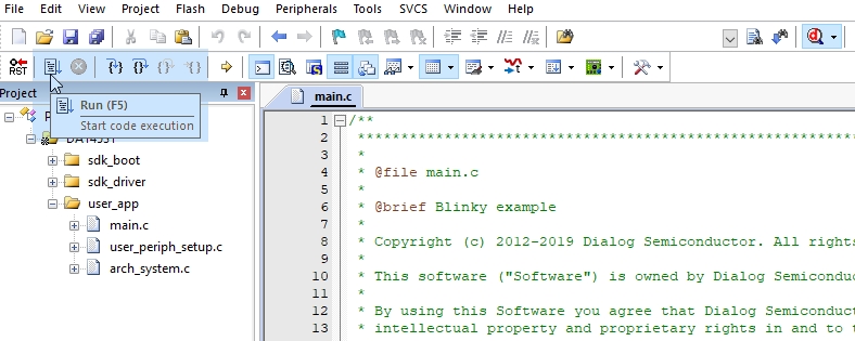
Figure 34 Blinky project: Code execution
When you see that the blinky message is displayed on your UART terminal screen and the orange LED is blinking, it means that you have successfully programmed and started the blinky program on the DA14535 Demo Board. The expected result on serial port can bee seen in the following figure:
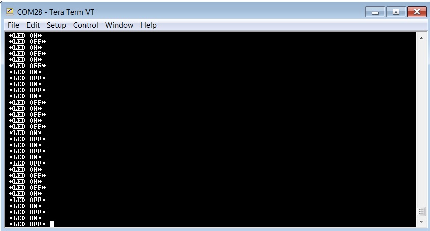
Figure 35 Tera Term terminal
SPI Flash Programming
The whole application here is placed/executed in RAM. It can also use SPI Flash to download an image file (.hex or .bin). The SmartSnippets™ Toolbox can be used to download code and erase flash via Serial Wire Debug Port (SWD).You can find more information in Appendices.
7.2. The Barebone BLE Example Application
The Barebone BLE example application demonstrates basic BLE procedures such as advertising, connection, updating connection parameters, and implementation of the Device Information Service Server (DISS). For more information, see the Bluetooth SIG.
Open the folder with the SDK files. This is the folder where you extracted the SDK zip file.
In
<sdk_root_directory>\projects\target_apps\ble_examples\ble_app_barebone\Keil_5, double-clickble_app_barebone.uvprojxto open the project in Keil®.
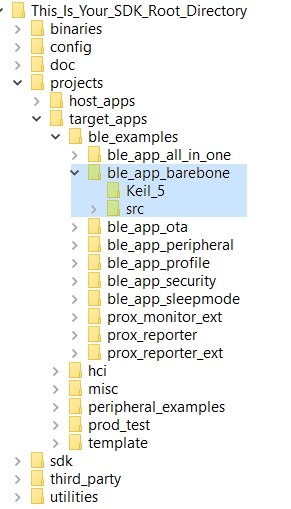
Figure 36 Barebone BLE project directory
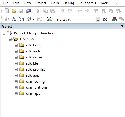
Figure 38 Barebone BLE: Keil® Project layout DA14535
To execute the code and run the example, repeat steps 3 to 14 in The Blinky Peripheral Example Application.
The barebone application does not use the UART (steps 9, 10, and 11 from Blinky can be skipped) and so the only jumpers required are those for the debugger interface as mentioned in Table 7.
Use the SmartBond app to scan for, and connect to the DLG-BRBN app, see Figure 39.
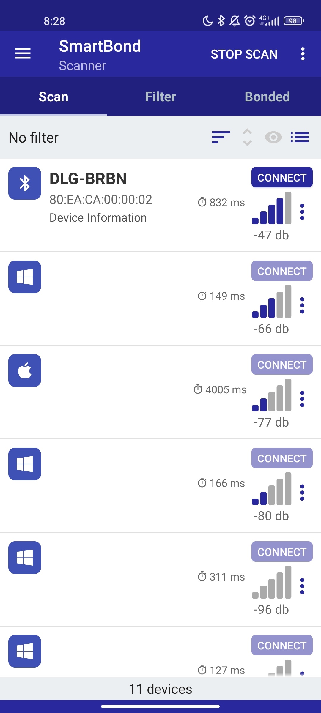
Figure 39 Using the SmartBond app to connect to the BLE application
Your BLE application is now running and advertising with the default advertiser string: DLG-BRBN.
Note
When you change the advertising name of your device and you leave the BD address the same, it will not show the update on your iPhone/iPad and not to connect to it anymore. It is easy to make your device forget about it. Follow some easy steps mentioned in the Apple Support Communities and your iPhone will not remember the Bluetooth device. If you change your mind, then you can pair the device as though it were new.
Bluetooth Device Address
When multiple devices use the same BD address in the same room test (close enough so both can be detected by the user’s Bluetooth explorer tool), it is highly recommended to change the BD address manually or use the static random address (advanced) to avoid any conflict. See DA145XX Tutorial BLE Advertising.
7.3. Troubleshooting
If there is any problem in connecting DEVKT-P Motherboard to the PC, here are some hints and possible solutions:
Make sure that your FTDI drivers are up to date. Drivers are available from the FTDI website
Use a different USB cable to rule out that a USB cable causes any issues
Connect the two elements to a different USB port on the host PC.
If you cannot see any blinky messages in your UART terminal and the LED is not blinking, check the UART and LED jumper configuration. See Table 9. The DA14531 has two different UART options: UART2 with 2 wires and UART2 with 1 wire.
If you cannot start a debug session, check the SWD debugger jumper configuration. See Table 7.
JTAG |
Function |
Jumper |
|---|---|---|
SWDIO |
SWD IO |
Connect J1.23 - J1.24 |
SWCLK |
SWD CLK |
Connect J1.21 - J1.22 |
Unlike DA14531 DEVKIT-P in DA143x DEVKIT-P, J8[1-2] is not user jumper (J8 is the reset sourced from the RA4M2). To activate a cursor during capturing session on the power profiler (for instance during connect, scan, disconnect) in SmartSnippets™ toolbox, you have 8 options to choose from on J24 (SW_trigger functionality). While getting a capture on the SmartSnippets™ toolbox, make sure to configure J9 as PMM (both J9[1-2] & J9[3-4] should be close).
If you have trouble with the J-link firmware or any issue with SDK operation, see DA1458x/68x Development Kit J-Link Interface Application Note AN-B-052.
When the device is programmed with an application in sleep mode to attach the debugger, use a lower speed in JLink, for example, 2000 Khz.
Note
If none of these actions resolved the issue, please contact the Renesas Forums OR BLE wireless connectivity in the Renesas Engineering community.
7.4. What is the Next ?
This tutorial does not cover all the topics relevant to software development environments. It describes the first steps necessary to get started with the Pro Development Kit. The following links provide more information on DA14535:
Renesas BLE Wiki page: Renesas Bluetooth Low Energy MCU Wiki.
UM-B-119: DA1453x/DA1458x SDK 6 Software Platform Reference: To know more about the software architecture.
DA1453x/DA14585x Sleep modes Tutorial: To learn more about DA14531 Power management.
AN-B-072 Booting Options on DA1453x : To learn more about the Booting Sequence for DA1453x.
UM-B-169 DA14535 Devkit Pro Hardware User Manual : To learn more about the hardware of the DA14535 development kit.
AN-B-098 DA14535 Hardware guidelines : To learn more about schematic, circuit explanation, and design guidelines for BLE applications based on the DA14531 SoC.