6. Appendix
6.1. Booting from Serial Interfaces
The DA1453x/DA1458x can boot from external serial devices when the OTP memory is not programmed. This is to enable the development of application code. At power-up the system enters Development Mode, where the boot code decides which interface to boot from. This section describes the boot sequence for all supported serial interfaces and provides the developer with the necessary information to realize the protocol required to establish communication between an external device and the DA1453x/DA1458x.
Note
For more information about booting the DA1453x/DA1458x, see the respective datasheets.
6.1.1. Introduction
The DA1453x/DA1458x operates in two modes: Normal mode and Development mode. The decision which mode the chip enters after power-up, is taken by the boot code that resides in the ROM. A complete flow chart of the boot code is illustrated in:
Figure 78 for DA14585
Figure 79 for DA14586
Figure 80 for DA14531-00, DA14531-01 and DA14530
Figure 81 for DA14535
The boot ROM code reads the Application Programmed flags from the OTP header to identify whether the chip is in Development mode or Normal mode.
Note
DA1458x: The OTP memory contains all zeros if not programmed.
DA1453x: The OTP memory contains all ones if not programmed.
If the predefined value is identified, then this ensures that the OTP memory is functional and that the application code is programmed. However, if the predefined value is not identified, either the OTP memory is not programmed (blank) or is not operational (random data).
When in Development mode, the boot ROM code initializes all serial peripheral devices from which the DA1453x/DA1458x might download code. The options are:
UART
SPI (both master and slave)
I2C (only master)
The boot ROM code searches for a valid response on various combinations of I/Os one after the other. There is also the option that the user can define desired I/Os with the use of a specific OTP field for the SPI interface.
The boot pins and serial peripherals search sequence are presented in the following section.
6.1.2. Boot Pins and Serial Peripherals Search Sequence
The DA1453x/DA1458x boot pins and serial peripherals search sequence are presented in Table 19, Table 20 and Table 21 Table 22
Interface |
Signal |
Step A |
Step B |
Step C |
Step D |
|---|---|---|---|---|---|
SPI Master |
SCK |
P0_0 |
P0_0 |
||
CS |
P0_3 |
P0_1 |
|||
MISO |
P0_6 |
P0_2 |
|||
MOSI |
P0_5 |
P0_3 |
|||
UART |
TX |
P0_0 |
P0_2 |
P0_4 |
P0_6 |
RX |
P0_1 |
P0_3 |
P0_5 |
P0_7 |
|
Baud Rate |
57600 / 8-N-1 |
115200 / 8-N-1 |
57600 / 8-N-1 |
9600 / 8-N-1 |
|
SPI Slave |
SCK |
P0_0 |
|||
CS |
P0_3 |
||||
MOSI |
P0_6 |
||||
MISO |
P0_5 |
||||
I2C |
SCL |
P0_0 |
P0_2 |
P0_4 |
P0_6 |
SDA |
P0_1 |
P0_3 |
P0_5 |
P0_7 |
Sequence |
Action |
|---|---|
0 |
SPI Master Step A |
1 |
SPI Master Step B |
2 |
UART Step A |
3 |
UART Step B |
4 |
UART Step C |
5 |
UART Step D |
6 |
SPI Slave Step A |
7 |
I2C Step A |
8 |
I2C Step B |
9 |
I2C Step C |
10 |
I2C Step D |
Step 1: Boot from external SPI master |
Step 2: Boot from 1-wire UART (first option) |
Step 3: Boot from 1-wire UART (second option) |
Step 4: Boot from 2-wire UART |
Step 5: Boot from external SPI slave |
Step 6: Boot from I2C |
|
|---|---|---|---|---|---|---|
P0_0/RST |
MISO |
Tx |
MOSI |
|||
P0_1 |
MOSI |
Rx |
SCS |
|||
P0_2 |
||||||
P0_3 |
SCS |
RxTx |
MISO |
SDA |
||
P0_4 |
SCK |
SCK |
SCL |
|||
P0_5 |
RxTx (default) |
|||||
P0_6 |
||||||
P0_7 |
||||||
P0_8 |
||||||
P0_9 |
||||||
P0_10 |
||||||
P0_11 |
Step 1: Boot from external SPI master |
Step 2: Boot from 1-wire UART (first option) |
Step 3: Boot from 1-wire UART (second option) |
Step 4: Boot from 2-wire UART |
Step 5: Boot from 2-wire UART |
Step 6: Boot from external SPI slave |
Step 7: Boot from I2C |
|
|---|---|---|---|---|---|---|---|
P0_0/RST |
MISO |
Tx |
MOSI |
||||
P0_1 |
MOSI |
Tx |
Rx |
SCS |
|||
P0_2 |
|||||||
P0_3 |
SCS |
RxTx |
Rx |
MISO |
SDA |
||
P0_4 |
SCK |
SCK |
SCL |
||||
P0_5 |
RxTx (default) |
||||||
P0_6 |
|||||||
P0_7 |
|||||||
P0_8 |
|||||||
P0_9 |
|||||||
P0_10 |
|||||||
P0_11 |
At each step, the boot ROM code sends a certain character to the peripheral controller and waits for an answer. If no answer is received within a certain amount of time, a timeout instructs the code to continue to the next step. If a response is detected, a specific protocol is executed and communication between the DA1453x/DA1458x and the external serial device is established. The code is downloaded from the external serial device to DA1453x/DA1458x RAM.
6.1.3. Boot Sequence
The boot sequence of DA14585 is shown in Figure 78.

Figure 78 DA14585 Boot Sequence
The boot sequence of DA14586 is shown in Figure 79.

Figure 79 DA14586 Boot Sequence
The boot sequence of DA14531-00, DA14531-01 and DA14530 booting is shown in Figure 80.

Figure 80 DA14531-00, DA14531-01 and DA14530 Boot Sequence
The boot sequence of DA14535 is shown in Figure 81.

Figure 81 DA14535 Boot Sequence
6.1.4. DA1453x/DA1458x Boot Protocols
6.1.4.1. Boot from SPI Bus - DA1453x/DA1458x Act as SPI Slave
The boot ROM code initially configures the DA1453x/DA1458x SPI controller with the following parameters:
8 bit mode
Slave role
Mode 0: SPI clock is initially expected to be low and SPI phase is zero.
The protocol required to establish a successful communication and to download the SW into the RAM is given in Table 23.
Note
The master SPI device generates the SPI clock for the DA1458x. In case of a continuous SPI clock, the frequency of this clock must not be higher than 500 kHz. For an SPI clock frequency higher than 500 kHz, the SPI clock should be paused after each byte.
Byte nr. |
DA1453x/DA1458x MOSI |
DA1453x/DA1458x MISO |
|---|---|---|
0 |
Preamble: 0x70 |
|
1 |
Preamble: 0x50 |
|
2 |
Empty: 0x00 |
|
3 |
Length LS byte |
Preamble ACK: 0x02 Preamble NACK:0x20 |
4 |
Length MS byte |
|
5 |
checksum byte |
|
6 |
Mode byte |
Length ACK:0x02 Length NACK:0x20 |
7 |
Empty: 0x00 |
|
8 |
Data bytes |
Code/Mode ACK:0x02 Code/Mode NACK:0x20 |
The external SPI master device starts by sending the Preamble bytes (0x70 and 0x50) followed by a zero byte. The DA1453x/DA1458x confirms the reception of the Preamble with 0x02 (Acknowledged) or 0x20 (Not Acknowledged) in case something went wrong. Bytes 3 and 4 define the length of the payload to follow. The least significant byte is sent first. The length is a number that represents the amount of data in 32-bit words.
Next, the SPI master must send the calculated checksum of the payload. The checksum is calculated by XORing every successive byte with the previous value. Initial checksum value is 0xFF.
Byte 6 defines the mode of operation directed by the SPI master (8, 16 or 32-bit modes) while the DA1453x/DA1458x SPI slave answers with ACK/NACK regarding the reception of the length bytes. The mode is encoded as follows:
0x00 = 8-bit mode
0x01 = 16-bit mode
0x02 = 32-bit mode
0x03 = Reserved
Byte 8 is the last control byte, where DA1453x/DA1458x replies with ACK/NACK with regard to the reception of the checksum and the mode, while the external SPI master starts to send the first byte of the payload (least significant byte of the first word).
The data section is presented in Table 24, and takes into consideration the instructed mode. The stream of data is followed by 2 extra empty slots to provide the required time to the DA1453x/DA1458x SPI controller to compute the checksum and answer with ACK/NACK.
Upon completion of the SPI master process, all related pads are set to input and pulled down.
Slot nr. |
MOSI (8-bit mode) |
MOSI (16-bit mode) |
MOSI (32-bit mode) |
MISO |
|---|---|---|---|---|
0 |
byte 0 |
byte 1, byte 0 |
byte 3, byte 2, byte 1, byte 0 |
|
1 |
byte 1 |
byte 3, byte 2 |
byte 7, byte 6, byte 5, byte 4 |
|
… |
||||
4*Len-1 or 2*Len-1 or Len-1 |
byte (4*Len–1) |
16-bit word (2*Len-1) |
32-bit word (Len-1) |
|
all 0x00 |
all 0x00 |
all 0x00 |
all 0xAA |
|
all 0x00 |
all 0x00 |
all 0x00 |
ACK: 0x02 NACK: 0x20 |
|
6.1.4.2. Booting from UART
The boot ROM code initially configures the DA1453x/DA1458x UART controller with the following parameters:
Bits: 8
No parity
1 stop bit
Baud rate: fixed at 115.2 Kbps for DA1453x, variable for DA1458x (see Table 19).
The protocol required to establish successful communication and to download the SW image into the RAM is shown in the next tables depending on the chip:
DA1458x
Table 25 Boot Protocol Byte nr.
DA1458x TX
DA1458x RX
0
STX = 0x02
1
SOH = 0x01
2
LEN_LSB byte (Basic)
3
LEN_MSB byte (Basic)
4
LEN_LSB byte (Extended)
5
LEN_MSB byte (Extended)
6
ACK = 0x06 or NACK = 0x15
7 to N
SW code bytes
N+1
checksum
N+2
ACK = 0x06
The protocol starts with the DA1458x UART TX pin that transmits 0x02 (Start TX - STX).
The external device is expected to answer with a 0x01 (Start of Header - SOH).
If the Basic LEN_LSB and LEN_MSB bytes are both zero, then the SW image is equal to or over 64 KByte. The following two Extended LEN_LSB and LEN_MSB bytes define the additional image length over the 64 KByte boundary. In that case the length of the downloaded SW image is calculated by the following formula:
length = 64 KByte + additional length defined by Extended LEN_MSB and LEN_LSB bytes.
The DA1458x answers with 0x06 (ACK) if the 5 bytes have been received and SOH has been identified, or answers with 0x15 (NACK) if anything went wrong.
If at least one of the Basic LEN_LSB or LEN_MSB byte is NOT zero, then the SW image is lower than 64 KByte. These bytes define the length of the downloaded SW image.
The DA1458x answers with 0x06 (ACK) if the 3 bytes have been received and SOH has been identified, or answers with 0x15 (NACK) if anything went wrong.
DA1453x
Table 26 Boot Protocol Byte nr.
DA1453x TX
DA1453x RX
0
STX = 0x02
1
SOH = 0x01
2
LEN_LSB byte
3
LEN_MSB byte
4
ACK = 0x06 or NACK = 0x15
5 to N
SW code bytes
N+1
checksum
N+2
ACK = 0x06
The protocol starts with the DA1453x UART TX pin that transmits 0x02 (Start TX - STX). The external device is expected to answer with a 0x01 (Start of Header - SOH) byte followed by 2 more bytes (LEN_LSB, LEN_MSB), which define the length of the code to be downloaded (first byte is the least significant, second the most significant). The DA1453x answers with 0x06 (ACK) if the 3 bytes have been received and SOH has been identified, or answers with 0x15 (NACK) if anything went wrong.
At this point the connection has been successfully established and the SW code will start to be downloaded. The next N bytes are received and put into the RAM, and starts at address 0x07FC0000 as shown in Table 27.
Address |
Byte 3 (MSB) |
Byte 2 |
Byte 1 |
Byte 0 (LSB) |
|---|---|---|---|---|
0x07FC0000 |
Code byte 3 |
Code byte 2 |
Code byte 1 |
Code byte 0 |
0x07FC0004 |
… |
… |
Code byte 5 |
Code byte 4 |
Upon completion of the required code bytes, the boot code calculates the checksum and send it over the URX. The boot sequence ends when the value 0x06 (ACK) is read at the URX line. checksum is calculated by XORing every successive byte with the previous value. The initial checksum value is 0x00.
At the final step of the boot code, the SYS_CTRL_REG register is programmed to:
Remap to address zero for execution to RAM (SYS_CTRL_REG[REMAP_ADR0] = 0x2)
Apply a SW reset, so the system starts to execute code at the remapped address (SYS_CTRL_REG[SW_RESET] = 0x1)
6.1.4.3. Booting from SPI Bus - DA1453x/DA1458x acting as SPI Master
The boot code configures the SPI with the following parameters:
8 bit mode
Master role
Mode 3: SPI clock is initially high and SPI phase is shifted by 90 degrees.
The SPI clock frequency is set by default at 2 MHz.
The protocol required to establish a successful communication and to download the SW image into the RAM is shown in the next tables, and depend on the chip:
DA1458x as SPI master
Table 28 Boot Protocol Byte nr.
DA1458x MOSI
DA1458x MISO
0
Read command
1
Address byte 0 = 0x00
2
Address byte 1 = 0x00
3 to N
Dummy bytes = 0x00
N+1
‘p’ = 0x70
N+2
‘P’ = 0x50
N+3 to N+5
Dummy bytes
N+6
Length extension byte
N+7
LEN_MSB byte
N+8
LEN_LSB byte
N+9 …
Code bytes
If Length Extension byte is equal to one, then the SW downloaded image size will be equal to or over 64 KByte. The image length is calculated based on the following formula:
length = 64 KByte + additional length defined by LEN_MSB and LEN_LSB bytes.
If Length Extension byte is NOT equal to one, then the SW downloaded image size will be lower than 64 KByte. The image length is defined by the LEN_MSB and LEN_LSB bytes.
DA1453x as SPI master
Table 29 Boot Protocol Byte nr.
DA1453x/DA1458x MOSI
DA1453x/DA1458x MISO
0
Read command
1
Address byte 0 = 0x00
2
Address byte 1 = 0x00
3 to N
Dummy bytes = 0x00
N+1
‘p’ = 0x70
N+2
‘P’ = 0x50
N+3 to N+6
Dummy bytes
N+7
LEN_MSB byte
N+8
LEN_LSB byte
N+9 …
Code bytes
The image length is defined by the LEN_MSB and LEN_LSB bytes.
The sequence as described in Table 28 or Table 29 is repeated for 4 different cases regarding the Read command and the Dummy byte parameters as indicated in Table 30.
Case nr. |
Read command opcode |
Number of dummy bytes |
|---|---|---|
0 |
0x03 |
0 |
1 |
0x03 |
1 |
2 |
0x0B |
2 |
3 |
0xE8 |
5 |
Note
The length of the SW image is received after the 4th Read command is issued (opcode = 0xE8).
As soon as the length has been received (2 bytes - LEN_MSB and LEN_LSB), the actual code download into RAM starts. The start address is the base address of the RAM. The byte alignment is according to Table 27.
During the final step of the boot code a SW reset is given and the system starts to execute the downloaded code.
6.1.4.4. Booting from I2C Bus - DA1453x/DA1458x Acting as I2C Master
The boot code initializes the I2C controller in master mode with the following parameters:
I2C slave address = 0x50 (7-bit address)
I2C speed to standard mode (100 kbit/s)
The boot code initially scans to find an I2C slave device at addresses 0x50 up to 0x57. After a successful slave address identification, a specific protocol is executed to download the SW into the RAM as shown in the next tables. There is a specfic table per chip. If unsuccessful, a timeout is programmed to expire after 20 ms to get the chip out of the I2C booting mode and into the next one.
DA1458x as I2C master
Table 31 Boot Protocol Byte nr.
DA1458x SDA
Action ( DA1458x I2C master)
0
0x70
Read command
1
0x50
Read command
2
LEN_MSB byte (Basic)
3
LEN_LSB byte (Basic)
4
- checksum over code
only
(image < 64KByte)
Read command
5
LEN_MSB byte (Extended)
6
LEN_LSB byte (Extended)
7
- checksum over code
only
(image >= 64KByte)
Read command
8 to 31
Dummy
Read command
32 to Length+32
Code data
Read command
If the Basic LEN_LSB and LEN_MSB bytes are both zero, then the SW image is equal to or over 64 KByte. The following two Extended LEN_LSB and LEN_MSB bytes define the additional image length over the 64 KByte boundary. In that case the length of the downloaded SW image is calculated by the following formula:
length = 64KByte + additional length defined by Extended LEN_MSB and LEN_LSB bytes.
Byte-4 shall be 1. Byte-7 inlcudes the checksum byte (calculated over code only).
If at least one of the Basic LEN_LSB or LEN_MSB byte is NOT zero, then the SW image is lower than 64 KByte. These bytes define the length of the downloaded SW image.
Byte-4 includes the checksum byte (calculated over code only).
DA1453x as I2C master
Table 32 Boot Protocol - DA1453x as I2C master Byte nr.
DA1453x SDA
Action ( DA1453x I2C master)
0
0x70
Read command
1
0x50
Read command
2
LEN_MSB byte
Read command
3
LEN_LSB byte
Read command
4
- checksum over code
only
Read command
5 to 31
Dummy
Read command
32 to Length+32
Code data
Read command
The boot code will calculate the checksum by XORing every successive byte with the previous value. Initial checksum value is 0x00. The checksum is calculated on multiples of 32 bytes. Padding with zeros is required when the payload size is not a multiple of 32 bytes.
At the final step of the boot code a SW reset is given and the system starts to execute the downloaded code.
6.2. Creation of a Secondary Bootloader
This section describes the implementation steps for the development of a secondary bootloader application for the DA1453x/DA1458x.
6.2.1. Introduction
The secondary bootloader is used in order to provide the users with a bigger flexibility so that they can customize their product’s booting procedure. Compared to the ROM booter, the secondary bootloader may be used in order to additionally support booting multi images and therefore enable the device to support SUOTA. The secondary bootloader in general supports either booting from external SPI or I2C slave peripherals (such as external SPI Flashes or I2C EEPROMs) and/or booting from serial peripherals such as the UART peripheral.
In both cases the image will be transferred from either of the aforementioned interfaces to RAM in order to be executed. The secondary bootloader can support booting encrypted and/or signed images. For that reason, there is a reserved OTP area which is located right above the OTP CS area or the OTP Header (for DA14585/DA14586 ICs). In the case of such encrypted and/or signed images the bootloader expects the keys for decryption and/or verification to be written by the user in that area so that these can be later used while booting to decrypt and/or verify the image.
Each encrypted and or signed image carries information about which keys will decrypt and/or verify it. More specifically, a total number of 5 decryption keys and 5 verification keys are supported. When an image is copied from UART or SPI/I2C to RAM for decryption and/or verification, it should carry information about which key (out of the 5 AES keys) decrypts it and which key(out of the 5 ECC keys) verifies it. These keys can also be revoked ONLY in the case of the external memory booting and ONLY if the image is signed, which means an image may also carry information about which keys it should revoke.
An extension of the secondary bootloader based on dual images is also presented in this section. The dual image bootloader is a building block for a Software Update Over The Air (SUOTA) enabled application. Finally the secondary bootloader code structure, the steps to test it and a methodology to measure the boot time are presented.
It is recommended to read Appendix Section 6.1, which describes the boot procedures supported by the DA1453x/DA1458x ROM code.
6.2.2. Boot from UART (Either 1-wire UART or 2-wire UART):
The bootloader may boot from the UART peripheral.
#define UART_SUPPORTED
will enable UART booting from 2-wire UART (da145xxx_config_basic.h)
#define ONE_WIRE_UART_SUPPORTED
will enable UART booting from 1-wire UART (da145xxx_config_basic.h)
That means that it can support downloading an image from UART directly to RAM. Depending on the image type, the image should be provided in different formats:
For a simple binary(non-encrypted and not signed) the user should build their application code and download the bare binary through UART.
The bootloader supports booting encrypted and/or signed images from UART. A raw binary image can be encrypted and/or signed with the mkimage tool. The resulting image is an image (same as a SUOTA single image) that has an image header that carries information about the image and which keys decrypt it (if it is encrypted) and/or verify it (if it is signed).
These configuration settings are included in the da145xxx_config_basic.h.
#define AES_ENCRYPTED_IMAGE_SUPPORTED (1)
Will make the bootloader support only encrypted images
#define SECURE_BOOT_ECC_IMAGE_SUPPORT (1)
Will make the bootloader support only signed images
Both the above macros can be defined simultaneously. In that case the bootloader will assume that only encrypted AND signed images are downloaded through UART. These images are expected to be first encrypted and THEN signed by the mkimage tool.
6.2.3. Boot from External Memory (Either via SPI or via I2C)
The bootloader can boot from an external SPI or I2C memory, These configuration settings are included in the da145xxx_config_basic.h.
#define SPI_FLASH_SUPPORTED
Will enable booting from an external SPI Flash
#define I2C_EEPROM_SUPPORTED
will enable booting from an external I2C EEPROM
By default the secondary bootloader will support booting multi images (a pair of single images - with image headers- along with a product header created by the mkimage tool).
The images can be plainly generated by the mkimage tool without any encryption or signing or they can be encrypted and/or signed
#define AES_ENCRYPTED_IMAGE_SUPPORTED (1)
Will make the bootloader support only encrypted images
#define SECURE_BOOT_ECC_IMAGE_SUPPORT (1)
Will make the bootloader support only signed images
Both the above macros can be defined simultaneously. In that case the bootloader will assume that only encrypted AND signed images are downloaded through the SPI or I2C memory. These images are expected to be first encrypted and THEN signed by the mkimage tool.
The bootloader supports key revokation ONLY when booting images from an external SPI or I2C memory. For key revokation to be supported, the image has to be first successfully verified so that the we know that the image requesting a key revokation is an image that was created from a “trusted” source. That means that key revokation can only be performed by signed images.
For increased security against malicious images, the user may define the following in bootloader.h
#define INVALIDATE_BAD_IMAGES (1)
This will make sure that if a bad or invalid image is found in the SPI flash /I2C EEPROM after SUOTA, its image header will be invalidated/erased. This will ensure that in the next SUOTA session, this invalidated image bank will be prioritized for SUOTA instead of the other “good” image bank.
A bad image is an image that has an invalid image header, or has failed to be verified (during image verification in the case of signed images support), or after decryption the image’s CRC does not align with the CRC of its header.
Together with the new SUOTA secure features, where only one SUOTA session is allowed per boot, an attacker will not be able to brick the device by filling both image banks with a bad/malicious image.
6.2.4. OTP Key Storage
The OTP Key Storage of the secondary bootloader is an area in the OTP where the bootloader assumes that Decryption and Verification keys are stored. Currently up to 5 Decryption keys are supported and up to 5 ECC/Verification keys are supported. For all the DA453x ICs, the key storage area is right above the OTP CS area. For DA14585/DA14586 the key storage area is above the OTP Header area. The structure and addresses of the Key storage can be seen below:
6.2.4.1. The key storage is summarized below for each platform:
Target chip / Key |
DA14531 / DA14531-01 |
DA14585 / DA14586 |
DA14535/DA14533 |
|---|---|---|---|
AES Keys and IV storage area |
7F87CC8 |
7F8FBD0 |
7F82CC8 |
ECC keys storage area |
7F87D68 |
7F8FC70 |
7F82D68 |
AES Revokation area |
7F87EA8 |
7F8FDB0 |
7F82EA8 |
ECC Revokation area |
7F87EBC |
7F8FDD8 |
7F82EBC |
6.2.4.2. AES IV and Keys Storage area
The table below is shown the AES IV and Keys Storage area which is the area where 5 initialization vectors and keys are supposed to be written during production so that the bootloader can later use these pairs to decrypt downloaded images.
Target chip / Key |
DA14531 / DA14531-01 |
DA14585 / DA14586 |
DA14535/DA14533 |
|---|---|---|---|
AES Key and IV Entry 0 |
7F87CC8 |
7F8FBD0 |
7F82CC8 |
AES Key and IV Entry 1 |
7F87CE8 |
7F8FBF0 |
7F82CE8 |
AES Key and IV Entry 2 |
7F87D08 |
7F8FC10 |
7F82D08 |
AES Key and IV Entry 3 |
7F87D28 |
7F8FC30 |
7F82D28 |
AES Key and IV Entry 4 |
7F87D48 |
7F8FC50 |
7F82D48 |
6.2.4.3. AES Key and IV Entry format
Each AES and Key entry consists of an Initialization Vector and an AES key.
AES Key |
AES IV |
|---|---|
16 bytes |
16 bytes |
6.2.4.4. ECC Keys storage area
This is the area where 5 ECC public keys should be written during production. These keys will later be used from the secondary bootloader to verify any incoming images.
Target chip / Key |
DA14531 / DA14531-01 |
DA14585 / DA14586 |
DA14535/DA14533 |
|---|---|---|---|
ECC key entry 0 |
7F87D68 |
7F8FC70 |
7F82D68 |
ECC key entry 1 |
7F87DA8 |
7F8FCB0 |
7F82DA8 |
ECC key entry 2 |
7F87DE8 |
7F8FCF0 |
7F82DE8 |
ECC key entry 3 |
7F87E28 |
7F8FD30 |
7F82E28 |
ECC key entry 4 |
7F87E68 |
7F8FD70 |
7F82E68 |
6.2.4.5. ECC key entry
Each ECC key entry consists of a 64-byte ECC public key
ECC Public Key |
|---|
64 bytes |
6.2.4.6. AES Revokation area
This area is written by the bootloader if signed or signed and encrypted image requests to revoke a certain AES key and IV entry. It should not be touched during production. Key revokation is only supported when booting an image from an external memory and only if the image is signed.
Target chip / Key |
DA14531 / DA14531-01 |
DA14585 / DA14586 |
DA14535/DA14533 |
|---|---|---|---|
AES Revokation Flag 0 |
7F87EA8 |
7F8FDB0 |
7F82EA8 |
AES Revokation Flag 1 |
7F87EAC |
7F8FDB8 |
7F82EAC |
AES Revokation Flag 2 |
7F87EB0 |
7F8FDC0 |
7F82EB0 |
AES Revokation Flag 3 |
7F87EB4 |
7F8FDC8 |
7F82EB4 |
AES Revokation Flag 4 |
7F87EB8 |
7F8FDD0 |
7F82EB8 |
6.2.4.7. ECC revokation area
This area is written by the bootloader if a signed image requests to revoke a certain ECC key. It should not be touched during production. Key revokation is only supported when booting an image from an external memory and only if the image is signed.
Target chip / Key |
DA14531 / DA14531-01 |
DA14585 / DA14586 |
DA14535/DA14533 |
|---|---|---|---|
ECC Revokation Flag 0 |
7F87EBC |
7F8FDD8 |
7F82EBC |
ECC Revokation Flag 1 |
7F87EC0 |
7F8FDE0 |
7F82EC0 |
ECC Revokation Flag 2 |
7F87EC4 |
7F8FDE8 |
7F82EC4 |
ECC Revokation Flag 3 |
7F87EC8 |
7F8FDF0 |
7F82EC8 |
ECC Revokation Flag 4 |
7F87ECC |
7F8FDF8 |
7F82ECC |
When a key is revoked, the bootloader will not use that specific key anymore. Any downloaded images that request a revoked key to be used for their their verification and/or decryption will be considered invalid/bad and won’t be booted.
6.2.5. Application Description
6.2.5.1. File Structure
The file structure of the secondary_bootloader project is shown in Figure 82.

Figure 82 Secondary Bootloader File Structure
Initialization files and scatter-loading description files are in folder utilities/secondary_bootloader/startup:
bootloader_585_armclang.sct: The scatter-loading description file for DA1458x
bootloader_531_armclang.sct: The scatter-loading description file for DA14531-00, DA14531-01 and DA14530
bootloader_535_armclang.sct: The scatter-loading description file for DA14535
ldscript_DA14531.lds.S: The linker script file for DA14531-00, DA14531-01 and DA14530
ldscript_DA14535.lds.S: The linker script file for DA14535 and DA14533
ldscript_DA14585_586.lds.S: The linker script file for DA1458x
Application (*.c) files are in folder utilities/secondary_bootloader/src:
main.c: Contains the main function, the system initialization function and the main loop of the application
bootloader.c: Contains the functions to boot from SPI and EEPROM and the implementation of the dual image bootloader
uart_booter.c: Contains the functions to boot from UART
decrypt Contains the software implementation of the AES decryption
user_periph_setup Peripherals setup and initialization
ecc_verify.c: Contains the ECC Verify functions for secondary bootloader
key_storage.c: This is the Key Storage management file
otp_utils.c: This file contains the OTP useful functions
Application (*.h) files are in folder utilities/secondary_bootloader/includes:
sdk_defs.h: Contains some memory configuration settings. Also contains the
SDK_SEC_BOOTLOADER_LOAD_IMAGE_SIZE_INIT_VALUEconfiguration macro which is described here Figure 83.periph_setup.h: Contains the configuration settings for the peripherals (UART, SPI, SPI Flash) used by the secondary bootloader application.
bootloader.h: Contains the application configuration settings. For details see section Section 6.2.5.2.
da1458x_config_basic.h: Splits into da14585_config_basic.h, da14531_config_basic.h and da14535_config_basic.h and holds various configuration settings for the respective device.
ecc_verify.h: Header file for the ECC verification functions.
key_storage.h: Contains the configuration settings for the Key Storage management source file.
otp_utils.h: Header file for the OTP useful functions.
decrypt.h Contains the configuration settings for the software implementation of the AES decryption.
uart_booter.h: Contains configuration settings for bootting from UART
Driver (*.c) files for the peripheral interfaces are in folder sdk/platform/driver/. Detailed information about the drivers can be found in the API documentation.
sdk/platform/driver/spi/spi_58x.c: Driver for the SPI interface of DA1458x Soc
sdk/platform/driver/spi/spi_531.c: Driver for the SPI interface of DA1453x Soc
sdk/platform/driver/i2c/i2c.c: Driver for the I2C interface
sdk/platform/driver/spi_flash/spi_flash.c: Driver for an external SPI Flash memory
sdk/platform/driver/gpio/gpio.c: Driver for the GPIO interface
sdk/platform/driver/dma/dma.c: Driver for the DMA interface
6.2.5.2. Other Compilation and Configuration Settings
Some other compilation and configuration settings are included in these header files located under includes folder, Figure 82.
sdk_defs.h
The secondary bootloader application is usually copied and executed in the last RAM addresses.
This is in order to have space at the beginning of RAM to copy and execute the user’s application (copy from Flash/EEPROM to RAM, or copy from UART to RAM).
Configuration macro SDK_SEC_BOOTLOADER_LOAD_IMAGE_SIZE_INIT_VALUE defines the size of the available RAM space that can be used to copy and execute an image.
The default value of this macro is set to 0x9500 which is about 38144 bytes.
If the developers enable more features on the secondary bootloader side(thus increasing the secondary bootloader’s binary size), then they should consider decreasing the effective available RAM size (decrease the value of SDK_SEC_BOOTLOADER_LOAD_IMAGE_SIZE_INIT_VALUE).

Figure 83 SDK_SEC_BOOTLOADER_LOAD_IMAGE_SIZE_INIT_VALUE macro
Note
For DA1453x P0_0 is used for UART_TX. At the end of firmware download hardware reset functionality on P0_0 is enabled. External application should drive P0_0 to low to avoid hardware reset of the device.
The configuration settings for the peripherals are contained in header file periph_setup.h.
// Select EEPROM characteristics
#define I2C_EEPROM_DEV_SIZE   0x20000           // EEPROM size in bytes
#define I2C_EEPROM_PAGE_SIZE   256               // EEPROM page size in bytes
#define I2C_SLAVE_ADDRESS 0x50              // Set slave device address
#define I2C_SPEED_MODE    I2C_SPEED_FAST    // Speed mode: I2C_SPEED_STANDARD (100 kbits/s), I2C_SPEED_FAST (400 kbits/s)
#define I2C_ADDRESS_MODE  I2C_ADDRESSING_7B // Addressing mode: {I2C_ADDRESSING_7B, I2C_ADDRESSING_10B}
#define I2C_ADDRESS_SIZE  I2C_2BYTES_ADDR   // Address width: {I2C_1BYTE_ADDR, I2C_2BYTES_ADDR, I2C_3BYTES_ADDR}

// SPI Flash settings
// SPI Flash Manufacturer and ID
#define W25X10CL_MANF_DEV_ID   (0xEF10)    // W25X10CL Manufacturer and ID
#define W25X20CL_MANF_DEV_ID   (0xEF11)    // W25X10CL Manufacturer and ID
#define MX25R2035F_MANF_DEV_ID (0xC212)    // MX25R2035F Manufacturer and ID

// SPI Flash options
#define W25X10CL_SIZE   131072            // SPI Flash memory size in bytes
#define W25X20CL_SIZE   262144            // SPI Flash memory size in bytes
#define MX25R2035F_SIZE 262144            // SPI Flash memory size in bytes
#define W25X10CL_PAGE   256               // SPI Flash memory page size in bytes
#define W25X20CL_PAGE   256               // SPI Flash memory page size in bytes
#define MX25R2035F_PAGE 256               // SPI Flash memory page size in bytes

#if !defined (__DA14586__)
#define SPI_FLASH_DEV_SIZE          (256 * 1024)
#endif

//SPI initialization parameters
#define SPI_WORD_MODE  SPI_8BIT_MODE
#define SPI_SMN_MODE   SPI_MASTER_MODE
#define SPI_POL_MODE   SPI_CLK_INIT_HIGH
#define SPI_PHA_MODE   SPI_PHASE_1
#define SPI_MINT_EN    SPI_NO_MINT
#if !defined (__DA14531__)
#define SPI_CLK_DIV    SPI_XTAL_DIV_2
#endif

// UART GPIOs assignment
#if defined (__DA14531__)
#define UART_GPIO_PORT       GPIO_PORT_0
#define UART_TX_PIN          GPIO_PIN_0
#define UART_RX_PIN          GPIO_PIN_1
#define UART_FRAC_BAUDRATE   UART_BAUDRATE_115200
#else
#define UART_GPIO_PORT       GPIO_PORT_0
#define UART_TX_PIN          GPIO_PIN_4
#define UART_RX_PIN          GPIO_PIN_5
#define UART_FRAC_BAUDRATE   UART_BAUDRATE_57600
#endif

// SPI GPIO assignment
/****************************************************************************************/
/* SPI configuration                                                                    */
/****************************************************************************************/
// Define SPI Pads
#if defined (__DA14531__)
#if !defined (__FPGA__)
    #define SPI_EN_PORT             GPIO_PORT_0
    #define SPI_EN_PIN              GPIO_PIN_1

    #define SPI_CLK_PORT            GPIO_PORT_0
    #define SPI_CLK_PIN             GPIO_PIN_4

    #define SPI_DO_PORT             GPIO_PORT_0
    #define SPI_DO_PIN              GPIO_PIN_0

    #define SPI_DI_PORT             GPIO_PORT_0
    #define SPI_DI_PIN              GPIO_PIN_3
#else
    #define SPI_EN_PORT             GPIO_PORT_0
    #define SPI_EN_PIN              GPIO_PIN_11

    #define SPI_CLK_PORT            GPIO_PORT_0
    #define SPI_CLK_PIN             GPIO_PIN_7

    #define SPI_DO_PORT             GPIO_PORT_0
    #define SPI_DO_PIN              GPIO_PIN_9

    #define SPI_DI_PORT             GPIO_PORT_0
    #define SPI_DI_PIN              GPIO_PIN_10
#endif

#elif !defined (__DA14586__)
    #define SPI_EN_PORT             GPIO_PORT_0
    #define SPI_EN_PIN              GPIO_PIN_3

    #define SPI_CLK_PORT            GPIO_PORT_0
    #define SPI_CLK_PIN             GPIO_PIN_0

    #define SPI_DO_PORT             GPIO_PORT_0
    #define SPI_DO_PIN              GPIO_PIN_6

    #define SPI_DI_PORT             GPIO_PORT_0
    #define SPI_DI_PIN              GPIO_PIN_5
#endif

// EEPROM GPIO assignment
// Define I2C Pads
#define I2C_SCL_PORT                GPIO_PORT_0
#define I2C_SCL_PIN                 GPIO_PIN_2

#define I2C_SDA_PORT                GPIO_PORT_0
#define I2C_SDA_PIN                 GPIO_PIN_3
W25X10CL SPI Flash memory devices are supported. The W25X10CL arrays are organized into 512 programmable pages of 256 bytes each. Up to 256 bytes can be programmed at a time. The W25X10CL has 32 erasable sectors of 4 kB, 4 erasable 32 kB blocks and 2 erasable 64 kB blocks respectively. W25X20CL SPI Flash memory devices are also supported.
Other SPI Flash memory types can be supported if the above configuration settings (SPI_FLASH_DEFAULT_SIZE, SPI_FLASH_DEFAULT_PAGE, etc.) are changed.
GPIO Port 0 is used by default as it is supported by all DA1458x (WLCSP34, QFN40 and QFN48) and DA1453x (WLCSP17 and FCGQFN24) packages.
6.2.6. System Initialization
The secondary bootloader application executes in the retention memory, and allows the application code to be loaded into the System RAM. The secondary bootloader does the following actions:
In the main function, the secondary bootloader reloads the Watchdog timer with the max value and configures the Watchdog timer to trigger a HW reset upon expiration.
SetBits(WATCHDOG_CTRL_REG, NMI_RST, 1);    // WDOG will generate HW reset upon expiration
SetWord16(WATCHDOG_REG, 0xFF);             // Reset WDOG
SetWord16(RESET_FREEZE_REG, FRZ_WDOG);     // Start WDOG
Initializes the system.
system_init();
Boots from UART if the UART boot option is enabled and the UART RX pin is logic HIGH. Otherwise boots from SPI or I2C.
6.2.7. Getting Started
This section describes how to program the secondary bootloader into the OTP memory, program an application example (integrated processor Proximity Reporter) into the SPI Flash memory and measure the system’s boot time. A comparison with a normal booter (ROM booter in Development Mode) is also provided.
The SmartSnippets Toolbox provides tools for external SPI Flash and OTP memory programming.
6.2.7.1. Building the Application and Secondary Bootloader Images
Build the Proximity Reporter application image for DA14585 target to generate the executable file prox_reporter_585.hex.
Build the secondary bootloader image for the same target according to the following steps:
Open the Secondary Bootloader project:
For Keil 5:
\utilities\secondary_bootloader\secondary_bootloader.uvprojx.
Configure the project according to section Section 6.2.5.2.
Compile the project to generate the executable file secondary_bootloader_585.hex. This file is in directory
<utilities\secondary_bootloader\out_DA14585\Objects.
6.2.7.2. Writing Application HEX File into SPI Flash Memory
The SmartSnippets SPI Flash Programmer tool is used to download an application image file to an external SPI Flash memory connected to DA1453x/DA1458x.
The following instructions demonstrate how to do this with SmartSnippets Toolbox in UART mode when a DA14585 device is connected.
Open SmartSnippets and select the chip version.

Figure 84 Select Chip Version
Open the Board Setup tool and select the appropriate UART and SPI flash pin configuration as shown in Figure 85.

Figure 85 Board Setup
Open the SPI Flash Programmer tool: Programmer –> Flash code, select the application image file and burn it at SPI flash memory offset 0. When asked whether to make the SPI Flash memory bootable, there are two options to consider depending on the chip version and bootloader configuration:
Bootable SPI Flash: SmartSnippets will automatically add an AN-B-001 header at offset 0 of the SPI flash memory. The secondary bootloader will copy only the number of bytes defined in the SPI Flash header.
Non-bootable SPI Flash: SmartSnippets will not add an AN-B-001 header at offset 0 of the SPI flash memory. The secondary bootloader will copy 32 KB from SPI Flash memory starting at offset 0x0. Using this setup the maximum boot time can be measured.

Figure 86 SPI Flash Programmer
6.2.7.3. Writing Bootloader HEX File into OTP Memory
The SmartSnippets OTP Programmer tool enables the download of default firmware into the System RAM and to write a user-defined HEX or BIN file into the OTP memory. The tool can be used to write a secondary bootloader in the OTP memory of a DA1453x/DA1458x.
The next steps are required to write the executable
secondary_bootloader_585.hex into OTP memory with SmartSnippets in
UART mode:
Open SmartSnippets and select the chip version as in Figure 84.
Open the Board Setup tool and select the appropriate UART as in Figure 85.
Open the OTP Programmer tool and select the image file to download.

Figure 87 OTP Programmer
Burn the
secondary_bootloader_585.hexinto the OTP memory at offset 0. Enable Application Flag 1 and Application Flag 2, set DMA Length (Length = size / 4) and burn theOTP header.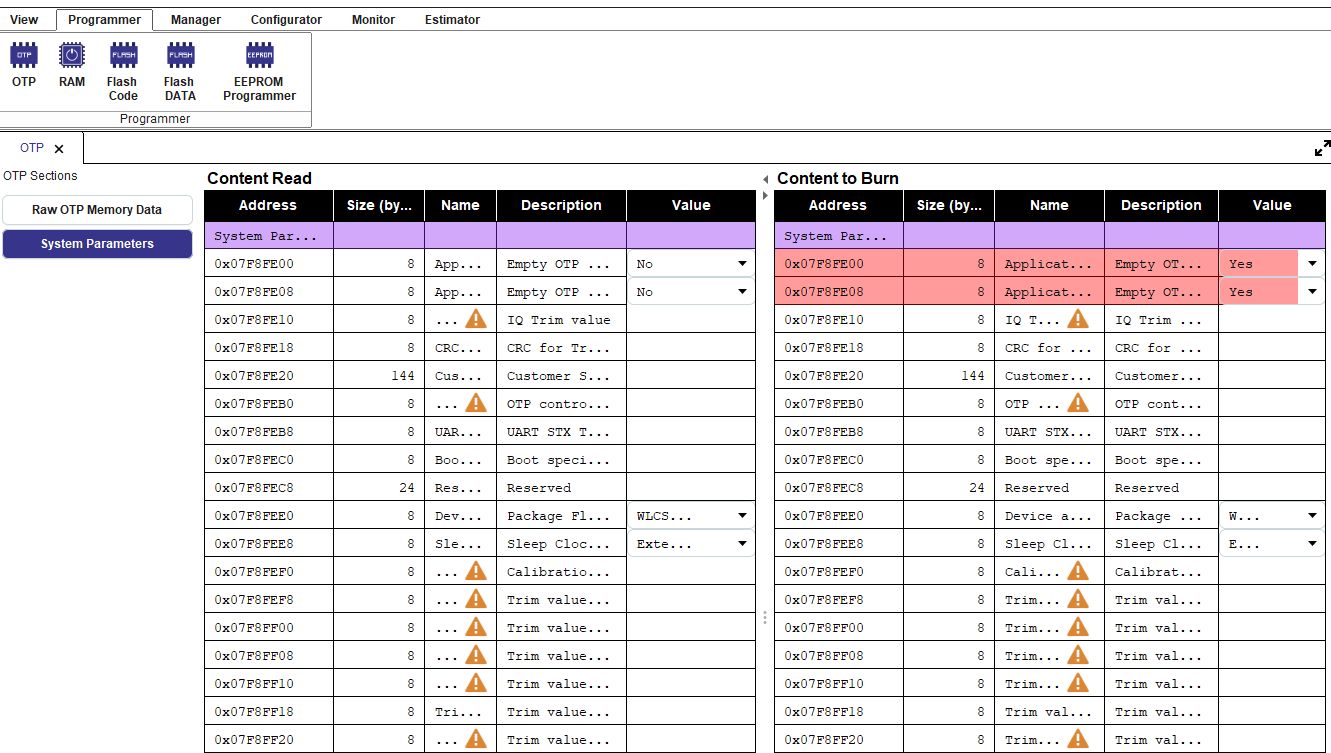
Figure 88 OTP Programmer
Note
For more info about SmartSnippets Toolbox, see the “SmartSnippets Toolbox, User manual”.
6.2.7.4. The mkimage Tool
The mkimage tool is used to create single (SUOTA) images. It is also used to created multi images (a pair of single images with a product header appended to them that is burned in the external memory to reserve the space needed to support SUOTA)
The tool supports two use cases:
Single image: Create a binary application image file (*.img), that contains both the application image header and the application firmware.
Multi-part image: Create the entire contents of the external non-volatile memory as a single multi-part binary image file (*.img), that can be written into a non-volatile memory with the SmartSnippets Toolbox.
The source code of the mkimage tool is in folder
\utilities\mkimage of the SDK.
6.2.7.4.1. Creating an Application Image File
The command line syntax to create an application image file (*.img) is:
Single image Creation
mkimage.exe single <in_file> <version_file> <out_file> [enc [<key> <iv>]]
singleInstructs the tool to create the <out_file> application image (*.img file).<infile>Specifies the raw application firmware binary file (.BIN file).<version_file>C header file that contains the version, time stamp and housekeeping information for the image header. It must be formatted similar to the SDK header filesdk\platform\include\sdk_version.h. It contains definitions such as:
#define SDK_VERSION "v_6.0.12.1020"
#define SDK_VERSION_DATE "2019-10-09 14:25 "
#define SDK_VERSION_STATUS "REPOSITORY VERSION v_6.0.12.1020"
This command can also create a single encrypted image by providing an AES key and AES IV that will be used to encrypt the image. The key and IV used here should also be burned in the OTP key storage to later be used by the secondary bootloader to successfully decrypt the image.
Apart from creating an encrypted single image, the key decryption info should also be written in the image’s header.
This can be achieved with the following command:
set the aes/iv key
mkimage.exe set_decryption_info file_to_modify aes_iv_key_index [aes_iv_revokation_index]
This command will be used to set the aes/iv key index in the image’s image header.
The first argument is the file that will be edited file_to_modify.
The second argument is the aes/iv key index that tells the bootloader which of the 5 OTP keys to use for decrypting the image aes_iv_key_index. The valid range for aes_iv_key_index is [0, 4].
The third argument aes_iv_revokation_index is optional and if provided it will write the image header with an AES/IV key revokation index, this will tell the bootloader which of the 5 AES/IV Key Entries should be revoked. The valid range for aes_iv_revokation_index is [0, 4]. .
Note
If key revokation is desired, the image should be signed afterwards. An unverified image cannot revoke a key. Also, key revokation is only supported by images coming from an external memory (SPI or I2C).
A new command has been added that supports single image signing. This means that before running the sign command, the mkimage single command has to be ran first.
Then the mkimage set_decryption_info command should be ran (if the image was encrypted) to set the decryption key information in the image header. As a last step before running the mkimage sign command, the user should also run the mkimage set_verification_info command to set the key verification index/info in the image’s header. Then after all these steps have been done the image can be signed. It is important to always sign the image as a last step after all the changes to image header have been done. The reason is because part of the image header is also used to sign the image.
set ECC key index
mkimage.exe set_verification_info <file_to_modify> ecc_key_index [ecc_revokation_index]
This command shall be used to set the ecc key index in the image’s header. The given ECC key index will tell the bootloader which of the 5 OTP ECC key entries should be used for verifying this image. The range of this value is 0 to 4.
The first argument is the file that will be edited file_to_modify.
The second argument is the ECC key index that tells the bootloader which of the 5 ECC OTP keys to use for verifying the image ecc_key_index.
The third argument ecc_revokation_index is optional and if provided it will write the image header with an ECC key revokation index. The valid range for ecc_revokation_index is [0, 4].
Note
If key revokation is desired, the image should be signed afterwards. An unverified image cannot revoke a key. Also, key revokation is only supported by images coming from an external memory.
Create sign image
mkimage.exe sign <input_image> <output_image> ecc_key
The input image’s name input_image should be provided followed by the output image’s name output_image.
the user should also provide the ECC private key ecc_key that should be used for signing. The key should be provided as a 64 hex string without any prefix (no 0x).
At the end of the signed image generation, the tool should print out the ECC private key, public key and signature so that the user is informed about all of them and also be able to use the public key on their application for verifying their singed images (burn it in the OTP Key storage along with other ECC public keys).
The resulting image is the given single image with its signature appended at the end of it (64 bytes).
Getting an ECC public key from a given ECC private key
mkimage.exe ecc_pubkey ecc_private_key
The user should provide their ECC private key ecc_private_key for which they want the ECC public key. The key should be provided as a 64 hex string without any prefix (no 0x).
The command should print out the ECC public key that is associated with the given private key.
Getting an ECC private and public key pair
mkimage.exe ecc_keygen
Note
This is a helper command for generating ecc private keys along with their associated public keys. The users may use their own secure method for obtaining an ECC private key and use the ecc_pubkey command described above to obtain its associated public key
6.2.7.4.2. Image header
To support the new security features, the image header has been updated to include additional information:
Status code |
Description |
|---|---|
0 |
Signature (0x70 = ‘p’) |
1 |
Signature (0x51 = ‘Q’) |
2 |
Valid Flag |
3 |
Image ID |
4-7 |
Code Size |
8-11 |
CRC |
12-17 |
Version |
28-31 |
Timestamp |
32 |
Flags |
33 |
Encryption Pad |
34-39 |
Key information |
40-63 |
Reserved |
Bytes 0-1: Signature field that identifies this header as a single image header.
Byte 2: Image valid flag (0x00 invalid, 0xAA valid).
Byte 3: Image identifier.
Bytes 4-7: Size (in bytes) of the following image.
Bytes 8-11: CRC of image.
Bytes 12-27: Image version information (ASCII string).
Bytes 28-31: Image timestamp.
Byte 32: Flags (0x00 not signed or encrypted, 0x01 encrypted, 0x02 signed, 0x03 signed and encrypted).
Byte 33: Encryption pad: Information on the padding that was done during encryption.
Bytes 34-39: The key information (6 bytes total).
ECC key information
This is filled with the mkimage set_verification_info command
ECC key index (1 byte): The ECC key index in the OTP storage that should be used to verify this image
ECC revokation valid flag (1 byte): A flag that marks the ECC revokation index valid or not
ECC revokation index (1 byte): The ECC revokation index (the index of the ECC key entry that should be revoked in the OTP key storage)
AES key information
This is filled with the mkimage set_decryption_info command
AES key index (1 byte): The AES key index in the OTP storage that should be used to decrypt this image
AES revokation valid flag (1 byte): A flag that marks the AES revokation index as valid or not
AES revokation index (1 byte): The AES revokation index (the index of the AES key entry that should be revoked in the OTP key storage)
11/ Bytes 33-63: Reserved for future use.
6.2.7.4.3. mkimage example
Below it shows how an encrypted and signed image is created:
Create the single encrypted image
create an encrypted image with key 06a9214036b8a15b512e03d534120006 and IV 3dafba429d9eb430b422da802c9fac41
mkimage single rawfile.bin sdk_version.h my_image.img enc 06a9214036b8a15b512e03d534120006 3dafba429d9eb430b422da802c9fac41
Set the AES/IV key index that is going to be used for decrypting this image (let’s say that the key pair above was put at index 0 in our current example)
mkimage set_decryption_info my_image.img 0
Set the ECC key index that is going to be used for verifying this image (let’s say that the ECC public key that results from the ECC private key that we are going to sign the image with, is placed in the ECC key entry 1)
mkimage set_verification_info my_image.img 1
Sign the image with the private key that associates with the public key that was burned in ECC key Entry 1
mkimage sign my_image.img my_signed_encrypted_image.img C9AFA9D845BA75166B5C215767B1D6934E50C3DB36E89B127B8A622B120F6721
This command will return the private ECC key that we used along with the ECC public key that results from that private key as well as the image’s signature:
Private Key:
c9afa9d845ba75166b5c215767b1d6934e50c3db36e89b127b8a622b120f6721
Public Key:
60fed4ba255a9d31c961eb74c6356d68c049b8923b61fa6ce669622e60f29fb67903fe1008b8bc99a41ae9e95628bc64f2f1b20c2d7e9f5177a3c294d4462299
Signature:
585c2dcf99ed6538f7292b1de70f9963a716b4d572ac11063cc86c65e7c465eb39a5dbfb629f014b977224750bd57f93c9d0087a9cd41410a10d2b5fe9648e15
The ECC public key should be written in the device’s OTP in the ECC key entry 1.
6.2.7.4.4. Creating an Application Image File
The image created from the above example can either be boot from UART in the secondary bootloader or downloaded via SUOTA to the device (stored in an external memory) or can be used to create a multi image for the user to burn during production in their device’s SPI or I2C external memory: The command line syntax to create a multi-part binary image file (*.img) with the entire contents of a non-volatile memory is:
mkimage.exe multi spi|eeprom [<bloader>] <in_img1> <off1> <in_img2> <off2> <off3> [cfg off4[,bdaddr]] <out_file>
multi Instructs the tool to create the <out_file> binary image file
(*.img) with the entire contents of the SPI Flash memory (option: spi) or
the I2C EEPROM (option: eeprom).
The multi-part image consists of:
AN-B-001 header plus the bootloader firmware <bloader> at offset 0, if <bloader> is provided.
<img1> (*.img image) at offset <off1>
<img2> (*.img image) at offset <off2>
Product header at offset <off3>
mkimage multi spi my_signed_encrypted_image.img 0x0000 my_signed_encrypted_image.img 0x19000 0x38000 my_multi_signed_encrypted_image.bin
The cfg option configures the following product header fields:
The application specific ‘Configuration Offset’ is initialized from off4. If off4 is not provided, then the ‘Configuration Offset’ field shall be set to 0xFFFFFFFF.
The BD Address is initialized from ‘bdaddr’. If bdaddr is not provided, then the BD Address field shall be set to FF:FF:FF:FF:FF:FF. If bdaddr is provided, it is required that no space exists between off4, the comma character and the ‘bdaddr’.
The offsets can be given either as decimal or as hexadecimal numbers.
The BD address ‘bdaddr’ can be given as XX:XX:XX:XX:XX:XX where X is a hex digit. For example, 80:EA:CA:01:02:03.
6.3. Production Line Tool Reference CLI
6.3.1. Introduction
This section describes the reference command line interface (CLI) for the production test tool of DA1453x/DA1458x.
The tool is a Microsoft Windows command line program that enables communication over UART with a DA1453x/DA1458x device that runs the production test firmware.
The production test firmware is a special firmware that supports:
The Bluetooth SIG standardized receiver and transmitter test HCI commands.
Additional custom test HCI commands.
All test commands are also supported by the RF Master tool of the SmartSnippets Toolbox.
Dialog has also designed a production test and programming unit “PLT” that enables you to reduce cost and increase throughput in volume test & programming of units centred around the DA1453x/DA1458x family.
6.3.2. Getting Started
6.3.2.1. Precompiled Binaries
Precompiled binaries are provided for both the production test firmware and tool in the following SDK paths:
Firmware
For DA14585
<sdk_root_directory>\binaries\da14585\prod_test\prod_test_585.hex
<sdk_root_directory>\binaries\da14585\prod_test\prod_test_585.bin
<sdk_root_directory>\binaries\da14585\prod_test\prod_test_585_UART_P04_P05.hex
<sdk_root_directory>\binaries\da14585\prod_test\prod_test_585_UART_P04_P05.binFor DA14586
<sdk_root_directory>\binaries\da14586\prod_test\prod_test_586.hex
<sdk_root_directory>\binaries\da14586\prod_test\prod_test_586.bin
<sdk_root_directory>\binaries\da14586\prod_test\prod_test_586_UART_P04_P05.hex
<sdk_root_directory>\binaries\da14586\prod_test\prod_test_586_UART_P04_P05.binFor DA14531
<sdk_root_directory>\binaries\da14531\prod_test\prod_test_531.hex
<sdk_root_directory>\binaries\da14531\prod_test\prod_test_531.bin
<sdk_root_directory>\binaries\da14531\prod_test\prod_test_531_UART_P00_P01.hex
<sdk_root_directory>\binaries\da14531\prod_test\prod_test_531_UART_P00_P01.bin
<sdk_root_directory>\binaries\da14531\prod_test\prod_test_531_UART_P03.hex
<sdk_root_directory>\binaries\da14531\prod_test\prod_test_531_UART_P03.bin
<sdk_root_directory>\binaries\da14531\prod_test\prod_test_531_UART_P05.hex
<sdk_root_directory>\binaries\da14531\prod_test\prod_test_531_UART_P05.binFor DA14531_01
<sdk_root_directory>\binaries\da14531_01\prod_test\prod_test_531_01.hex
<sdk_root_directory>\binaries\da14531_01\prod_test\prod_test_531_01.bin
<sdk_root_directory>\binaries\da14531_01\prod_test\prod_test_531_01_UART_P00_P01.hex
<sdk_root_directory>\binaries\da14531_01\prod_test\prod_test_531_01_UART_P00_P01.bin
<sdk_root_directory>\binaries\da14531_01\prod_test\prod_test_531_01_UART_P03.hex
<sdk_root_directory>\binaries\da14531_01\prod_test\prod_test_531_01_UART_P03.bin
<sdk_root_directory>\binaries\da14531_01\prod_test\prod_test_531_01_UART_P05.hex
<sdk_root_directory>\binaries\da14531_01\prod_test\prod_test_531_01_UART_P05.binFor DA14530
<sdk_root_directory>\binaries\da14530\prod_test\prod_test_530.hex
<sdk_root_directory>\binaries\da14530\prod_test\prod_test_530.bin
<sdk_root_directory>\binaries\da14530\prod_test\prod_test_530_UART_P00_P01.hex
<sdk_root_directory>\binaries\da14530\prod_test\prod_test_530_UART_P00_P01.bin
<sdk_root_directory>\binaries\da14530\prod_test\prod_test_530_UART_P03.hex
<sdk_root_directory>\binaries\da14530\prod_test\prod_test_530_UART_P03.bin
<sdk_root_directory>\binaries\da14530\prod_test\prod_test_530_UART_P05.hex
<sdk_root_directory>\binaries\da14530\prod_test\prod_test_530_UART_P05.binFor DA14535
<sdk_root_directory>\binaries\da14535\prod_test\prod_test_535.hex
<sdk_root_directory>\binaries\da14535\prod_test\prod_test_535.bin
<sdk_root_directory>\binaries\da14535\prod_test\prod_test_535_UART_P00_P01.hex
<sdk_root_directory>\binaries\da14535\prod_test\prod_test_535_UART_P00_P01.bin
<sdk_root_directory>\binaries\da14535\prod_test\prod_test_535_UART_P03.hex
<sdk_root_directory>\binaries\da14535\prod_test\prod_test_535_UART_P03.bin
<sdk_root_directory>\binaries\da14535\prod_test\prod_test_535_UART_P05.hex
<sdk_root_directory>\binaries\da14535\prod_test\prod_test_535_UART_P05.bin
Tool
<sdk_root_directory>\binaries\host\windows\prod_test_cmds\prod_test.exe
6.3.2.2. Building the Tool
For SDK 6.0.4 and above this is in: <sdk_root_directory>\utilities\prod_test\prod_test_cmds.
6.3.2.3. Building the Firmware
The required firmware is included in the SDK in folder:
(SDK 6.0.2 and later): <sdk_root_directory>\projects\target_apps\prod_test\prod_test
Steps to build the firmware
Open the folder
<sdk_root_directory>\projects\target_apps\prod_test\prod_test.Open the project.
Select menu
Project -> Rebuild all target filesto build the project.Get the generated hex file from the following folders:
For DA14585
.\Keil_5\out_DA14585\Objects
.\Keil_5\out_DA14585_UART_P04_P05\ObjectsFor DA14586
.\Keil_5\out_DA14586\Objects
.\Keil_5\out_DA14586_UART_P04_P05\ObjectsFor DA14531
.\Keil_5\out_DA14531\Objects
.\Keil_5\out_DA14531_UART_P00_P01\Objects
.\Keil_5\out_DA14531_UART_P03\Objects
.\Keil_5\out_DA14531_UART_P05\ObjectsFor DA14531_01
.\Keil_5\out_DA14531_01\Objects
.\Keil_5\out_DA14531_01_UART_P00_P01\Objects
.\Keil_5\out_DA14531_01_UART_P03\Objects
.\Keil_5\out_DA14531_01_UART_P05\ObjectsFor DA14535
.\Keil_5\out_DA14535\Objects
.\Keil_5\out_DA14535_UART_P00_P01\Objects
.\Keil_5\out_DA14535_UART_P03\Objects
.\Keil_5\out_DA14535_UART_P05\Objects
6.3.3. General Description
The general syntax of the tool is:
prodtest <switches> <command> <command-arg-1> … <command-arg-2>
A command always returns a status code and optionally a list of return values. The return status code and values are written to the standard output in a simple format: <value_name> = <value>.
The return status code is also returned as an exit code.
A zero status code represents the successful execution of a command. A non-zero status code encodes the type of failure.
All other output of the tool is written to stderr (except the help message when -h option is used).
6.3.4. Command Line Switches
6.3.4.1. Switch -h
Description: print out all the commands of prodtest on a command line terminal
Syntax: prodtest -h
6.3.4.2. Switch -p
Description: select the COM port number on a PC. All commands require this switch.
Syntax: prodtest -p <COM_PORT_NUMBER> ...
6.3.4.3. Switch -v
Description: display the tool’s version
Syntax: prodtest -v
6.3.5. Commands
6.3.5.1. cont_pkt_tx
Description: this is the Bluetooth SIG standardized HCI_LE_Transmitter_Test command. It continuously transmits packets until the stoptest command is executed.
Syntax: prodtest -p <COM_PORT_NUMBER> cont_pkt_tx <FREQUENCY> <DATA_LENGTH> <PAYLOAD_TYPE>
Parameters:
FREQUENCY is an even integer between 2402 and 2480. For example, integer 2480 corresponds to 2.480 GHz.
DATA_LENGTH is the payload length in bytes (a number between 37 and 255).
PAYLOAD_TYPE must have one of the following values:
0 : Pseudo-Random bit sequence 9
1 : Pattern of alternating bits '11110000'
2 : Pattern of alternating bits '10101010'
3 : Pseudo-Random bit sequence 15
4 : Pattern of All '1' bits
5 : Pattern of All '0' bits
6 : Pattern of alternating bits '00001111'
7 : Pattern of alternating bits '0101'
Example:
prodtest -p 14 cont_pkt_tx 2402 35 6
Output example:
status = 0
6.3.5.2. pkt_tx
Description: transmit the specified number of packets.
Syntax: prodtest -p <COM_PORT_NUMBER> pkt_tx <FREQUENCY> <DATA_LENGTH> <PAYLOAD_TYPE> <NUMBER_OF_PACKETS>
Parameters:
FREQUENCY is an even integer between 2402 and 2480. For example, 2480 corresponds to 2.480 GHz.
DATA_LENGTH is the payload length in bytes (a number between 37 and 255).
PAYLOAD_TYPE must have one of the following values:
0 : Pseudo-Random bit sequence 9
1 : Pattern of alternating bits '11110000'
2 : Pattern of alternating bits '10101010'
3 : Pseudo-Random bit sequence 15
4 : Pattern of All '1' bits
5 : Pattern of All '0' bits
6 : Pattern of alternating bits '00001111'
7 : Pattern of alternating bits '0101'
NUMBER_OF_PACKETS is an integer between 1 and 65535.
Example: the following command sends 1000 packets:
prodtest -p 14 pkt_tx 2402 35 6 1000
Output example:
status = 0
6.3.5.3. start_pkt_rx
Description: This is the Bluetooth SIG standardized HCI_LE_Receiver_Test command. It continuously receives packets until the stoptest command is executed.
Syntax: prodtest -p <COM_PORT_NUMBER> start_pkt_rx <FREQUENCY>
Parameters:
FREQUENCY is an even integer between 2402 and 2480. For example, 2480 corresponds to 2.480 GHz.
Example:
prodtest -p 14 start_pkt_rx 2402
Output example:
status = 0
6.3.5.4. start_pkt_rx_stats
Description: starts packet RX with additional statistics. It continuously receives packets until the stop_pkt_rx_stats command is executed.
Syntax: prodtest -p <COM_PORT_NUMBER> start_pkt_rx_stats <FREQUENCY>
Parameters:
FREQUENCY is an even integer between 2402 and 2480. For example, 2480 corresponds to 2.480 GHz.
Example:
prodtest -p 14 start_pkt_rx_stats 2402
Output example:
status = 0
6.3.5.5. stop_pkt_rx_stats
Description: ends packet RX with additional statistics and reports the following statistics:
number of packets received correctly (nb_packets_received_correctly)
number of packets with sync error (nb_packets_with_syncerror)
number of packets with checksum error (nb_packets_received_with_crcerr)
RSSI in dBm (rssi)
Syntax: prodtest -p <COM_PORT_NUMBER> stop_pkt_rx_stats
Example:
prodtest -p 14 stop_pkt_rx_stats
Output example:
status = 0
nb_packets_received_correctly = 8529
nb_packets_with_syncerror = 0
nb_packets_received_with_crcerr = 1
rssi = -37.30
6.3.5.6. stoptest
Description: This is the Bluetooth SIG standardized HCI_LE_Test_End command. It is used:
after a
cont_pkt_txcommand to end the standard packet TX test mode.after a
start_pkt_rxcommand to end the standard packet RX mode and report the number of received packets.
Syntax: prodtest -p <COM_PORT_NUMBER> stoptest
Example:
prodtest -p 14 stoptest
Output example (the number of packets is always zero when executed after a cont_pkt_tx):
status = 0
number_of_packets = 0
Output example (when executed after a start_pkt_rx):
status = 0
number_of_packets = 4360
6.3.5.7. unmodulated TX
Description: starts a Continuous Wave (CW) or unmodulated TX test.
Syntax: prodtest -p <COM_PORT_NUMBER> unmodulated TX <FREQUENCY>
Parameters:
FREQUENCY is an even integer between 2402 and 2480. For example, 2480 corresponds to 2.480 GHz.
Example:
prodtest -p 14 unmodulated TX 2404
Output example:
status = 0
6.3.5.8. unmodulated RX
Description: starts the unmodulated RX test.
Syntax: prodtest -p <COM_PORT_NUMBER> unmodulated RX <FREQUENCY>
Parameters:
FREQUENCY is an even integer between 2402 and 2480. For example, 2480 corresponds to 2.480 GHz.
Example:
prodtest -p 14 unmodulated RX 2404
Output example:
status = 0
6.3.5.9. unmodulated OFF
Description: stops unmodulated TX or RX test.
Syntax: prodtest -p <COM_PORT_NUMBER> unmodulated OFF
Example:
prodtest -p 14 unmodulated OFF
Output example:
status = 0
6.3.5.10. start_cont_tx
Description: starts the continuous TX test mode. It transmits continuously a modulated signal until the stop_cont_tx command is executed.
Syntax: prodtest -p <COM_PORT_NUMBER> start_cont_tx <FREQUENCY> <PAYLOAD_TYPE>
Parameters:
FREQUENCY is an even integer between 2402 and 2480. For example, 2480 corresponds to 2.480 GHz.
PAYLOAD_TYPE must have one of the following values:
0 : Pseudo-Random bit sequence 9
1 : Pattern of alternating bits '11110000'
2 : Pattern of alternating bits '10101010'
3 : Pseudo-Random bit sequence 15
4 : Pattern of All '1' bits
5 : Pattern of All '0' bits
6 : Pattern of alternating bits '00001111'
7 : Pattern of alternating bits '0101'
Example:
prodtest -p 14 start_cont_tx 2404 4
Output example:
status = 0
6.3.5.11. stop_cont_tx
Description: stops the continuous TX test mode.
Syntax: prodtest -p <COM_PORT_NUMBER> stop_cont_tx
Example:
prodtest -p 14 stop_cont_tx
Output example:
status = 0
6.3.5.12. reset
Description: this is the Bluetooth SIG standardized HCI_Reset command.
Syntax: prodtest -p <COM_PORT_NUMBER> reset
Example:
prodtest -p 14 reset
Output example:
status = 0
6.3.5.13. xtrim rd
Description: reads the value of the XTAL16M trimming register as specified in DA14585 and DA14586 datasheets: CLK_FREQ_TRIM_REG (0x50000002).
The value is reported in decimal format.
Syntax: prodtest -p <COM port number> xtrim rd
Example:
prodtest -p 14 xtrim rd
Output example:
status = 0
trim_value = 500
6.3.5.14. xtrim wr
Description: writes a value into the XTAL16M trimming register. The new value is written immediately and is already effective when the prodtest program finishes executing this command.
Syntax: prodtest -p <COM port number> xtrim wr <trim_value>
Parameters:
trim_value is the unsigned 16-bit decimal value to be written into the XTAL16M trimming register.
Example:
prodtest -p 14 xtrim wr 500
Output example:
status = 0
6.3.5.15. xtrim en
Description: enables XTAL16M output on GPIO P0_5. The command takes effect immediately.
Syntax: prodtest -p <COM port number> xtrim en
Example:
prodtest -p 14 xtrim en
Output example:
status = 0
Note
This command can also be used to enable the 32 kHz clock on a GPIO 0_6. To do this, two additional registers need to be set with the write_reg16 command (see section Section 6.3.5.29). Enable the 32 kHz clock in CLK_32K_REG, set bit 0 and bit 7 to ‘1’ Set GPIO P0_6 to output mode. In P06_MODE_REG, set bit 8 and 9 to ‘1’.
Example:
prodtest -p 14 write_reg16 50000020 079D
prodtest -p 14 write_reg16 50003012 0300
Output example:
status = 0
6.3.5.16. xtrim dis
Description: disables XTAL16M output on GPIO P0_5. The command takes effect immediately.
Note
This command also disables: XTAL32K output on GPIO P0_6 RC16M output on P0_7 RC32K output on P1_0.
Syntax: prodtest -p <COM port number> xtrim dis
Example:
prodtest -p 14 xtrim dis
Output example:
status = 0
6.3.5.17. xtrim inc
Description: increments the XTAL16M trimming register. The register’s new value is already effective when the prodtest program finishes the execution of this command.
Syntax: prodtest -p <COM port number> xtrim inc <delta>
Parameters:
delta is the unsigned 16-bit decimal value to be added to the XTAL16M trimming register.
Example:
prodtest -p 14 xtrim inc 5
Output example:
status = 0
6.3.5.18. xtrim dec
Description: decrements the XTAL16M trimming register. The register’s new value is already effective when the prodtest program finishes executing this command.
Syntax: prodtest -p <COM port number> xtrim dec <delta>
Parameters:
delta is the unsigned 16-bit decimal value to be subtracted from the XTAL16M trimming register.
Example:
prodtest -p 14 xtrim dec 5
Output example:
status = 0
6.3.5.19. xtrim cal
Description: runs the XTAL16M trimming register calibration procedure, which uses an externally applied 500 ms high square pulse as a reference for trim value calibration. The procedure executes the following steps:
Calibrates the XTAL16M trimming register.
Programs the calibrated value in OTP (at address 0x7F8C).
Enables the “XTAL16M trim value is valid” bit in OTP (at address 0x7F78).
If a square pulse has not been applied on the given GPIO then the calibration procedure will fail with a status code equal to 27.
Syntax: prodtest -p <COM port number> xtrim cal <Px_y>
Parameters:
Px_y is the GPIO that the external square pulse is applied on.
Example:
prodtest -p 14 xtrim cal P1_0
Output example:
status = 0
6.3.5.20. xtrim caltest
Description: behaves identically to “xtrim cal” with the exception that it does not modify the OTP.
Syntax: prodtest -p <COM port number> xtrim caltest <Px_y>
Parameters:
Px_y is the GPIO that the external square pulse is applied on.
Example:
prodtest -p 14 xtrim caltest P1_0
Output example:
status = 0
6.3.5.21. sleep
Description: puts the device to sleep for a specified number of minutes and seconds.
Syntax: prodtest -p <COM_PORT_NUMBER> sleep <mode> <minutes> <seconds>
Parameters:
mode is one of the following power modes:
"none" for Active Mode
"extended" for Extended Sleep Mode
"deep" for Deep Sleep Mode
minutes is a number between 0 and 255
seconds is a number between 0 and 255
If both minutes and seconds are set to zero, then the device sleeps forever. The active peripherals in each sleep mode are shown in Table 41 and Table 42.
Power mode |
PD_SYS |
PD_PER |
PD_DBG |
PD_RAD |
PD_SRx |
Analog |
|---|---|---|---|---|---|---|
Extended/Deep Sleep |
Auto OFF |
Programmable |
Auto OFF |
Programmable |
Programmable |
Auto OFF |
Power mode |
PD_SYS |
PD_AON |
PD_SLP |
PD_RAD |
PD_TIM |
|---|---|---|---|---|---|
|
Auto OFF |
ON |
ON |
OFF |
Programmable |
Known limitations:
UART communication is lost when the device wakes up from extended sleep mode
The device will not wake up from Extended sleep with OTP copy mode
Example 1:
prodtest -p 14 sleep none 1 0
Example 2:
prodtest -p 14 sleep extended 0 30
Example 3:
prodtest -p 14 sleep deep 0 0
Output example:
status = 0
6.3.5.22. otp wr_xtrim
Description: writes the XTAL16M trim value into the OTP header.
Syntax: prodtest -p <COM port number> otp wr_xtrim <decimal trim value>
Parameters:
Decimal trim value is the unsigned 16-bit decimal XTAL16M trim value to be written into the OTP header
Example:
prodtest -p 14 otp wr_xtrim 500
Output example:
status = 0
6.3.5.23. otp rd_xtrim
Description: reads the XTAL16M trim value from the OTP header. The output value is in decimal format.
Syntax: prodtest -p <COM port number> otp rd_xtrim
Example:
prodtest -p 14 otp rd_xtrim
Output example:
status = 0
otp_xtrim_value = 500
6.3.5.24. otp wr_bdaddr
Description: writes the Bluetooth Device address into the OTP header.
Syntax: prodtest -p <COM port number> otp wr_bdaddr <BD address>
Parameters:
BD address is the Bluetooth Device address to be written into the OTP header. The BD address must be formatted as XX:XX:XX:XX:XX:XX where X is a hexadecimal digit
Example:
prodtest -p 14 otp wr_bdaddr 44:49:41:4c:4f:47
Output example:
status = 0
6.3.5.25. otp_read
Description: reads consecutive words from OTP memory.
Syntax: prodtest -p <COM port number> otp_read <otp address> <word count>
Parameters:
otp address is the start address of the OTP memory region to be read. This is a word address and must therefore be divisible by 4. It must be lower than 0x8000. It must be formatted as a 16-bit hexadecimal number
Word count is the number of words to be read. The accepted range is from 1 to 60. The word count must satisfy the formula: <otp address> + 4 * <word count> <= 0x8000. It must be formatted as a decimal number
Example:
prodtest -p 16 otp_read 7FDC 5
Output example:
status = 0
[7FDC] = 1234A5A5
[7FE0] = A5A51234
[7FE4] = 14121117
[7FE8] = 24222127
[7FEC] = 00000007
6.3.5.26. otp_write
Description: writes consecutive words into OTP memory.
Syntax: prodtest -p <COM port number> otp_write <otp address> <word #1> ... <word #n>
Parameters:
otp address is the start address of the OTP memory region to be written. This is a word address and must therefore be divisible by 4. It must be lower than 0x8000. It must be formatted as a 16 bit hexadecimal number
Word #i is the word value to be written in address: <otp address> + 4 * i. It must be formatted as a 32 bit hexadecimal number. The number of word value arguments must be at most 60 and must satisfy the formula: <otp address> + 4 * n <= 0x8000
Example:
prodtest -p 16 otp_write 7FDC 1234A5A5 A5A51234
Output example:
status = 0
6.3.5.27. read_reg16
Description: reads the value of a 16-bit register. The output value is printed in hex.
Syntax: prodtest -p <COM port number> read_reg16 <register address>
Parameters:
register address is the address of the 16-bit register to be read. The register address must be half-word aligned, and must therefore be divisible by 2. It must be formatted as a 32-bit hexadecimal number
Example: the following command reads TRIM_CTRL_REG (0x50000016).
prodtest -p 16 read_reg16 50000016
Output example:
status = 0
value = 00A2
6.3.5.28. read_reg32
Description: reads the value of a 32-bit register. The output value is printed in hex.
Syntax: prodtest -p <COM port number> read_reg32 <register address>
Parameters:
register address is the address of the 32-bit register to be read. The register address must be word aligned and must therefore be divisible by 4. It must be formatted as a 32-bit hexadecimal number
Example: the following command reads PATCH_VALID_REG (0x40008400).
prodtest -p 16 read_reg32 40008400
Output example:
status = 0
value = 00000001
6.3.5.29. write_reg16
Description: writes into a 16-bit register.
Syntax: prodtest -p <COM port number> write_reg16 <register address> <register value>
Parameters:
register address is the address of the 16-bit register to be read. The register address must be half-word aligned and must therefore be divisible by 2. It must be formatted as a 32-bit hexadecimal number
register value is the value to be written into the register. It must be formatted as a 16-bit hexadecimal number
Example: the following command writes 0x00B3 in TRIM_CTRL_REG (0x50000016).
prodtest -p 16 write_reg16 50000016 00B3
Output example:
status = 0
6.3.5.30. write_reg32
Description: writes into a 32-bit register.
Syntax: prodtest -p <COM port number> write_reg32 <register address> <register value>
Parameters:
register address is the address of the 32-bit register to be read. The register address must be word aligned and must therefore be divisible by 4. It must be formatted as a 32-bit hexadecimal number
register value is the value to be written into the register. It must be formatted as a 32-bit hexadecimal number
Example: the following command writes 0x0000000F in PATCH_VALID_REG (0x40008400).
prodtest -p 16 write_reg32 40008400 0000000F
Output example:
status = 0
6.3.6. Return Status Codes
Table 43 summarizes the return codes of the production’s test tool.
Status code |
Description |
|---|---|
0 |
SC_NO_ERROR |
1 |
SC_MISSING_COMMAND |
2 |
SC_INVALID_COMMAND |
3 |
SC_WRONG_NUMBER_OF_ARGUMENTS |
4 |
SC_INVALID_COM_PORT_NUMBER |
5 |
SC_INVALID_FREQUENCY_ARG |
6 |
SC_INVALID_DATA_LENGTH_ARG |
7 |
SC_INVALID_PAYLOAD_TYPE_ARG |
8 |
SC_COM_PORT_INIT_ERROR |
9 |
SC_RX_TIMEOUT |
12 |
SC_INVALID_UNMODULATED_CMD_MODE_ARG |
13 |
SC_COM_PORT_NOT_SPECIFIED |
14 |
SC_INVALID_SLEEP_CMD_MODE_ARG |
15 |
SC_INVALID_SLEEP_CMD_MINUTES_ARG |
16 |
SC_INVALID_SLEEP_CMD_SECONDS_ARG |
17 |
SC_INVALID_XTAL_TRIMMING_CMD_OPERATION_ARG |
18 |
SC_INVALID_XTAL_TRIMMING_CMD_TRIM_VALUE_ARG |
19 |
SC_INVALID_OTP_CMD_OPERATION_ARG |
20 |
SC_INVALID_OTP_CMD_TRIM_VALUE_ARG |
21 |
SC_INVALID_OTP_CMD_BDADDR_ARG |
22 |
SC_INVALID_OTP_ADDRESS_ARG |
23 |
SC_INVALID_NUMBER_OF_OTP_WORDS_ARG |
24 |
SC_INVALID_WORD_VALUE_ARG |
25 |
SC_INVALID_GPIO_ARG |
26 |
SC_XTAL_TRIMMING_CAL_OUT_OF_RANGE_ERROR |
27 |
SC_XTAL_TRIMMING_CAL_FREQ_NOT_CONNECTED |
28 |
SC_INVALID_REGISTER_ADDRESS_ARG |
29 |
SC_INVALID_REGISTER_VALUE_ARG |
1000 - 1063 |
SC_HCI_STANDARD_ERROR_CODE_BASE (1000) + standard HCI error code |
6.4. Flash Programmer
6.4.1. Overview
Flash programmer (flash_programmer) is a target side application used to upload and read back the application code that runs on platforms powered by the DA1453x/DA1458x series integrated circuit. After the flash programmer application is booted, the platform communicates over the UART or JTAG interface with the host application that allows it to read or write application code to the FLASH, EEPROM or OTP memory. Both sides exchange messages that contain operation codes, statuses and payload with respect to the defined protocol.
6.4.2. Enhanced Flash Programmer Security in SDK 6.0.24
The
SECURE_AES_KEYS_IV_PROGRAMMERmacro inda1455xx_config_basic.hhas been introduced in SDK 6.0.24 to enhance cybersecurity.
This feature enables secure programming of AES keys and IVs, ensuring protection against unauthorized access.
/****************************************************************************************************************/
/* Enable the secure programming feature of the AES keys and IVs.                                               */
/* Users should also define their secret unwrapping operation and key                                           */
/****************************************************************************************************************/
#define SECURE_AES_KEYS_IV_PROGRAMMER               (0)
Two new commands have been added to the flash programmer to handle AES keys securely:
#define ACTION_OTP_SECURE_READ_ENC_KEYS  0xD0
#define ACTION_OTP_SECURE_WRITE_ENC_KEYS 0xD1
The ACTION_OTP_SECURE_WRITE_ENC_KEYS (0xD1) command is used to store wrapped AES keys in one step. The flash programmer checks if the correct key size is written, then unwraps the keys and saves them in a secure storage area (OTP). If everything works, it returns a success message; if not, it gives an error.
The ACTION_OTP_SECURE_READ_ENC_KEYS (0xD0) command reads the stored keys, wraps them again, and sends them securely back to the PLT.
This following image Figure 89 illustrates the secure method for reading and writing application code to FLASH/EEPROM memory using the Flash Programmer and the newly introduced Cybersecurity Mechanism in SDK 6.0.24. The flash programmer communicates with an external host via UART and interacts with the DA1453x/DA1458x BLE device. A Secure Secondary Bootloader has been introduced Section 6.2, supporting encrypted and/or signed images, with up to five decryption and five verification keys.

Figure 89 Enhanced Flash Programming with Cybersecurity in SDK 6.0.24
6.4.3. Communication Channel
The communication channel is selected at compile time and is limited to the following options:
6.4.3.1. UART (USE_UART Flag Defined)
In this mode, flash programmer receives messages from the host and responds back with the UART interface. It also defines an exchange buffer of size 64K- 1 bytes (0xFFFF) for DA14585/585 targets and 32K - 1 bytes (0x7FFF) for DA1453x. This limits the amount of data that can be written or read in a single message. This is the implication of the 2 byte wide length indicator that (along with the checksum) is sent before the actual message frame. The frame length and the checksum code are not cached inside the buffer and holds only the actual message (including possible headers and payload).
With this knowledge it is easy to figure out, that in case of the OTP write operation, the actual firmware chunk size is limited to 0xFFF8 (0xFFFF minus the 7 bytes of header data for this particular message) for DA1458x and 0x7FF8 for DA1453x. As communication via UART is synchronous, the defined buffer is used for both the incoming and the outgoing messages.
The flash programmer communicates by default with the host through pins P0_0, P0_1 at speed 57600 for DA1458x targets and at speed 115200 for DA1453x. This can be changed by appending to the binary 1 byte. This byte selects pins and baud rate according to the following table.
Platform |
Selector |
TX pin |
RX pin |
Baud rate |
|---|---|---|---|---|
DA1458x |
0 (default) |
P0_0 |
P0_1 |
57600 |
2 |
P0_2 |
P0_3 |
115200 |
|
4 |
P0_4 |
P0_5 |
57600 |
|
6 |
P0_6 |
P0_7 |
9600 |
|
DA1453x |
0 (default) |
P0_0 |
P0_1 |
115200 |
3 (single wire UART) |
P0_3 |
P0_3 |
115200 |
|
5 (single wire UART) |
P0_5 |
P0_5 |
115200 |
6.4.3.2. JTAG (No Flag Defined)
Uses shared memory for message exchange. The host application reads from and writes to a certain memory region with the JTAG interface. The Flash programmer constantly polls one of these regions for new messages and responds accordingly. There are two regions defined:
BASE_MEMORY - in this region messages and responses are stored
TARGET_MEMORY - in this region the payload is stored
The available message space is limited to 64K for DA1458x and to 32K for DA1453x (the limitations of the actual message headers also apply here. In case of write request, the offset field is 2 bytes wide which covers the first 64K/32K memory addresses).
Note
The message exchange protocol slightly differs in both cases and is described in another section.
6.4.4. Functionality
The Flash programmer supports the following operations:
hardware setup required to operate the FLASH, EEPROM, OTP peripherals (this includes enabling LDO and GPIO configuration)
reading the currently running flash programmer version
reading the requested amount of data from the application memory regions
writing the requested amount of data to the application memory regions
erasing the requested amount of data from the application memory regions (not supported by all non-volatile memory types)
6.4.5. Data Exchange Protocol
Flash programmer listens for host commands in an infinite loop. The host should receive a response for each of the issued actions. Those should be issued sequentially once the previous ones were completed by the target. This message exchange sequence is done differently for each of the supported exchange channels.
6.4.5.1. UART
The host sends a command packet through UART in the following form:
Len (16 bits) |
|
Op Code |
Address (32 bits) |
Length (16 bits) |
Data … |
|---|---|---|---|---|---|
HEADER SECTION |
MESSAGE SECTION |
||||
The first Len parameter is the total length of the message section, which starts with the Op Code (8 bits) and ends where the variable length Data buffer ends. checksum is also calculated for the message section. The message section length is limited by the 2 bytes wide Len.
The result response sent to the host varies from one message to the other. The exact request and response messages are presented later in this document but it is important to note that they do also have the header section that contain the Len and checksum fields.
Data is transferred over the wire with a network byte order (big endian).
6.4.5.2. JTAG (Memory Mapped API)
The host writes a message to the memory section to issue a command, which
starts at the address that is in the BASE_MEMORY variable. The message is structured
in the following form:
Memory offset |
Memory content |
Order |
|---|---|---|
ACTION_OFFSET |
Op Code |
LSB |
SIZE_OFFSET |
Length (16 bits) |
MSB |
SIZE_OFFSET + 1 |
LSB |
|
ADDRESS_OFFSET |
Address Offset (32 bits) |
|
ADDRESS_OFFSET + 1 |
||
ADDRESS_OFFSET + 2 |
MSB |
|
ADDRESS_OFFSET + 3 |
||
RESULT_OFFSET |
Result |
LSB |
ERROR_OFFSET |
Additional error code when Result is not ACTION_OK |
|
ERROR_OFFSET + 1 |
||
ERROR_OFFSET + 2 |
MSB |
|
ERROR_OFFSET + 3 |
Memory offset |
Memory content |
|---|---|
0 |
|
1 |
|
… |
Additionally the payload of Length is written into the Data
buffer pointed by the TARGET_MEMORY variable when applicable.
Note
The host writes the packet sections at certain offsets relative to the starting address that is saved in the BASE_MEMORY variable. Writing the Op Code should be the last step as this triggers the action on the target platform. The Op Code value changes back to 0 once the message is processed and the response in the Result section is filled. This way the host knows when to read the results of the triggered action. Similarly to the messages exchanged via UART the response structure depends on the command sent by the host.
For the DA1453x/DA1458x platform, memory addresses and offsets are set according to the following table:
Platform |
TARGET_MEMORY |
BASE_MEMORY |
ACTION_OFFSET |
SIZE_OFFSET |
ADDRESS_OFFSET |
RESULT_OFFSET |
|---|---|---|---|---|---|---|
DA1458x |
0x07FC8000 |
0x07FC7C00 |
0x00 |
0x02 |
0x04 |
0x08 |
DA1453x |
0x07FC4000 |
0x07FC3C00 |
0x00 |
0x02 |
0x04 |
0x08 |
Because of the nature of the JTAG interface, no endianness conversion is being done. Data should be written in the target platform’s endianness (little endian).
6.4.5.3. Handshake
The host application needs to receive a signal from the target to determine if the target is ready to receive requests. This is done differently for both communication channels:
UART:
Target sends the ‘’Hello’’ string over UART to report readiness.
JTAG:
Target sets the result status value to ACTION_READY at the
BASE_MEMORY + RESULT_OFFSET memory address. The host application can
monitor this memory address to detect flash_programmer readiness.
6.4.5.4. Messages
Note that the following list of messages do not list the header sections (Length, checksum), which is sent along every UART message that is exchanged over the protocol.
6.4.5.4.1. General
- ACTION_READ_VERSION
(0x10) - Reads the flash programmer application version
UART:
Table 49 UART_REQUEST Len
(16 bits)
- checksum
(32 bits)
Op Code
0x07
checksum
0x10
Table 50 UART_RESPONSE Len
(16 bits)
- checksum
(32 bits)
Op Code
0x0D
checksum
0x82
JTAG:
Table 51 Memory Layout at BASE_MEMORY Address Memory offset
Request memory content
Response memory content
ACTION_OFFSET
0x10 (ACTION_READ_VERSION)
0x00 (NO_ACTION)
SIZE_OFFSET
do not care
do not care
ADDRESS_OFFSET
do not care
do not care
RESULT_OFFSET
do not care
0x82 (ACTION_CONTENTS)
Table 52 Data Buffer Memory Layout at TARGET_MEMORY Address Memory offset
Request memory content
Response memory content
0
do not care
v
1
do not care
_
2
do not care
5
…
do not care
…
- ACTION_VPP_ENABLE
(0x50) - Enable the transistor that controls high voltage (6.8v) when OTP memory is written.
UART:
Table 53 UART_REQUEST Len
(16 bits)
- checksum
(32 bits)
Op Code (8 bits)
VPP_ENABLE (8 bits)
0x02
checksum
0x50
0x00 or 0x01
Table 54 UART_RESPONSE Len
(16 bits)
- checksum
(32 bits)
Status (8 bits)
0x01
checksum
0x83 (ACTION_OK) or 0x84 (ACTION_ERROR)
- ACTION_READY
(0x5A) - This is used only by firmware to inform the host that the target is ready to handle host requests when running in Shared Memory Mode (JTAG).
JTAG:
Table 55 Memory Layout at BASE_MEMORY Address Memory offset
Memory content when not ready
Memory content when ready
ACTION_OFFSET
do not care
do not care
SIZE_OFFSET
do not care
do not care
ADDRESS_OFFSET
do not care
do not care
RESULT_OFFSET
0x00
0x82 (ACTION_READY)
- ACTION_UART_GPIOS
(0x31) - Configure UART data lines. Returns ACTION_ERROR if pins are incorrect.
UART:
Table 56 UART_REQUEST Len (16 bits)
- checksum
(32 bits)
Op Code
TX_PORT
TX_PIN
RX_PORT
RX_PIN
0x05
checksum
0x31
0x00
0x04
0x00
0x05
Table 57 UART_RESPONSE Len (16 bits)
- checksum
(32 bits)
Status (8 bits)
0x01
checksum
0x83 (ACTION_OK) or 0x84 (ACTION_ERROR)
JTAG:
Unsupported
6.4.5.4.2. OTP Memory
- ACTION_OTP_READ
(0x80) - Read the requested amount of data from the OTP memory at the given offset.
UART:
Table 58 UART_REQUEST Len (16 bits)
- checksum
(32 bits)
Op Code
Address offset (32 bits)
Length (16 bits)
Len (16 bits)
checksum (32 bits)
0x07 + length
checksum
0x80
offset
length
0x07 + length
checksum
Table 59 UART_RESPONSE Len
(16 bits)
- checksum
(32 bits)
Status(8 bits)
Data …
0x01 + data length
checksum
0x82 (ACTION_CONTENTS)
read data
JTAG:
Table 60 Memory Layout at BASE_MEMORY Address Memory offset
Request memory content
Response memory content
ACTION_OFFSET
0x80 (ACTION_OTP_READ)
0x00 (NO_ACTION)
SIZE_OFFSET
data length
data length
ADDRESS_OFFSET
address offset
address offset
RESULT_OFFSET
do not care
0x82 (ACTION_CONTENTS)
Table 61 Data Buffer Memory Layout at TARGET_MEMORY Address Memory offset
Request memory content
Response memory content
0
do not care
data0
1
do not care
data1
2
do not care
data2
…
do not care
data3
- ACTION_OTP_WRITE
(0x81) - Write the requested amount of data into the OTP memory at the given offset.
UART:
Table 62 UART_REQUEST Len (16 bits)
- checksum
(32 bits)
Op Code
Address offset (32 bits)
Length (16 bits)
Data (LENGTH*8 bits)
0x07 + length
checksum
0x81
memory address
length
data to write
Table 63 UART_RESPONSE Len
(16 bits)
- checksum
(32 bits)
Status (8 bits)
Error Code (32 bits)
0x01 or 0x05
checksum
0x83 (ACTION_OK) or 0x84 (ACTION_ERROR)
Additional error code - only if Status is set to ACTION_ERROR.
JTAG:
Table 64 Memory Layout at BASE_MEMORY Address Memory offset
Request memory content
Response memory content
ACTION_OFFSET
0x81 (ACTION_OTP_WRITE)
0x00 (NO_ACTION)
SIZE_OFFSET
size
size
ADDRESS_OFFSET
address offset
address offset
RESULT_OFFSET
do not care
0x83 (ACTION_OK) or 0x84 (ACTION_ERROR)
ERROR_OFFSET
do not care
Error code (32 bits) - only if result is ACTION_ERROR
Table 65 Data Buffer Memory Layout at TARGET_MEMORY Address Memory offset
Request memory content
Response memory content
0
data0
data0
1
data1
data1
2
data2
data2
…
data3
data3
6.4.5.4.3. SPI FLASH
- ACTION_SPI_READ
(0x90) - Read the requested amount of data from the SPI FLASH memory at given memory address.
UART:
Table 66 UART_REQUEST Len (16 bits)
- checksum
(32 bits)
Op Code
Address offset (32 bits)
Length (16 bits)
Data (LENGTH*8 bits)
0x07 + length
checksum
0x90
memory address
length
data to write
Table 67 UART_RESPONSE Len (16 bits)
- checksum
(32 bits)
Status (8 bits)
Data…
0x01 + data length
checksum
0x82 (ACTION_CONTENTS)
read data
JTAG:
Table 68 Memory Layout at BASE_MEMORY Address Memory offset
Request memory content
Response memory content
ACTION_OFFSET
0x90 (ACTION_SPI_READ)
0x00 (NO_ACTION)
SIZE_OFFSET
data length
data length
ADDRESS_OFFSET
address
address
RESULT_OFFSET
do not care
0x82 (ACTION_CONTENTS)
Table 69 Data Buffer Memory Layout at TARGET_MEMORY Address Memory offset
Request memory content
Response memory content
0
do not care | data0
1
do not care | data1
2
do not care | data2
…
do not care | data3
- ACTION_SPI_WRITE
(0x91) - Write the requested amount of data into SPI FLASH memory at given offset.
UART:
Table 70 UART_REQUEST Len (16 bits)
- checksum
(32 bits)
Op Code
Address offset (32 bits)
Length (16 bits)
Data (LENGTH*8 bits)
0x07 + length
checksum
0x91
memory address
length
data to write
Table 71 UART_RESPONSE Len
(16 bits)
- checksum
(32 bits)
Status (8 bits)
Error Code (32 bits)
0x01 or 0x05
checksum
0x83 (ACTION_OK) or 0x84 (ACTION_ERROR)
Additional error code - only if Status is set to ACTION_ERROR.
JTAG:
Table 72 Memory Layout at BASE_MEMORY Address Memory offset
Request memory content
Response memory content
ACTION_OFFSET
0x91 (ACTION_FLASH_WRITE)
0x00 (NO_ACTION)
SIZE_OFFSET
size
size
ADDRESS_OFFSET
memory address
memory address
RESULT_OFFSET
do not care
0x83 (ACTION_OK) or 0x84 (ACTION_ERROR)
ERROR_OFFSET
do not care
Error code (32 bits) - only if result is ACTION_ERROR
Table 73 Data Buffer Memory Layout at TARGET_MEMORY Address Memory offset
Request memory content
Response memory content
0
data0
data0
1
data1
data1
2
data2
data2
…
data3
data3
- ACTION_SPI_ERASE
(0x92) - Erase SPI FLASH memory.
UART:
Table 74 UART_REQUEST Len (16 bits)
- checksum
(32 bits)
Op Code
0x01
checksum
0x92
Table 75 UART_RESPONSE Status (8 bits)
Error Code (32 bits)
Status (8 bits)
Error Code (32 bits)
0x01 or 0x05
checksum
0x83 (ACTION_OK) or 0x84 (ACTION_ERROR)
Additional error code - only if Status is set to ACTION_ERROR.
JTAG:
Table 76 Memory Layout at BASE_MEMORY Address Memory offset
Request memory content
Response memory content
ACTION_OFFSET
0x92 (ACTION_SPI_ERASE)
0x00 (NO_ACTION)
SIZE_OFFSET
Do not care
Do not care
ADDRESS_OFFSET
Do not care
Do not care
RESULT_OFFSET
Do not care
0x83 (ACTION_OK) or 0x84 (ACTION_ERROR)
ERROR_OFFSET
Do not care
Error code (32bits) - only if result is ACTION_ERROR
Note
Data buffer memory layout at TARGET_MEMORY address: Target memory is not used.
- ACTION_SPI_ID
(0x93) - Read flash JEDEC ID.
UART:
Table 77 UART_REQUEST Len (16 bits)
- checksum
(32 bits)
Op Code
0x01
checksum
0x93
Table 78 UART_RESPONSE Len (16 bits)
checksum (32bits)
Status
(8 bits)
MANUFACTU RER ID (8 bits)
JEDEC ID 1 (8 bits)
0x05
checksum
0x82 (ACTION_C ONTENTS)
0
id
id
JTAG:
Table 79 Memory Layout at BASE_MEMORY Address Memory offset
Request memory content
Response memory content
ACTION_OFFSET
0x93 (ACTION_EEPROM_READ)
0x00 (NO_ACTION)
SIZE_OFFSET
Do not care
Do not care
ADDRESS_OFFSET
Do not care
Do not care
RESULT_OFFSET
Do not care
0x82 (ACTION_CONTENTS)
Table 80 Data Buffer Memory Layout at TARGET_MEMORY Address Memory offset
Request memory content
Response memory content
0
Do not care
Device ID byte 2
1
Do not care
Device ID byte 1
2
Do not care
Manufacturer ID
3
Do not care
0
- ACTION_SPI_ERASE_BLOCK
(0x94) - Erase specified number of sectors starting from flash address.
UART:
Table 81 UART_REQUEST Len (16 bits)
- checksum
(32 bits)
Op Code
Address (32 bits)
Sectors (16 bits)
0x07
checksum
0x94
address
n
Table 82 UART_RESPONSE Len (16 bits)
checksum 32bits)
Status
(8 bits)
MANUFACTURER ID (8 bits)
JEDEC ID 1 (8 bits)
0x01 or 0x05
checksum
0x83 (ACTION_O K) or 0x84 (ACTION_E RROR)
Additiona l error code - only if Status is not set to ACTION_OK
0x01 or 0x05
checksum
JTAG:
Table 83 Memory Layout at BASE_MEMORY Address Memory offset
Request memory content
Response memory content
ACTION_OFFSET
0x94 (ACTION_SPI_ERASE_BLO CK)
0x00 (NO_ACTION)
SIZE_OFFSET
sector count
Do not care
ADDRESS_OFFSET
address
Do not care
RESULT_OFFSET
Do not care
0x83 (ACTION_OK) or 0x84 (ACTION_ERROR)
ERROR_OFFSET
Do not care
Error code - only if result is ACTION_ERROR
- ACTION_SPI_GPIOS
(0x95) - Configure SPI data lines. Returns ACTION_ERROR if any pin is incorrect.
UART:
Table 84 UART_REQUEST Len (16 bits)
- checksum
(32 bits)
Op Code
CS PORT
CS PIN
CLK PORT
CLK PIN
DO PORT
DO PIN
DI PORT
DI PIN
0x09
checksum
0x95
0x00
0x03
0x00
0x00
0x00
0x06
0x00
0x05
Table 85 UART_RESPONSE Len (16 bits)
- checksum
(32 bits)
Status
0x01
checksum
0x83 (ACTION_OK) or 0x84 (ACTION_ERROR)
JTAG:
Table 86 Memory Layout at BASE_MEMORY Address Memory offset
Request memory content
Response memory content
ACTION_OFFSET
0x95 (ACTION_SPI_GPIOS)
0x00 (NO_ACTION)
SIZE_OFFSET
Do not care
Do not care
ADDRESS_OFFSET
Do not care
Do not care
RESULT_OFFSET
Do not care
0x83 (ACTION_OK) or 0x84 (ACTION_ERROR)
Table 87 Data Buffer Memory Layout at TARGET_MEMORY Address Memory offset
Request memory content
Response memory content
0
0x00 (CS PORT)
Do not care
1
0x03 (CS PIN)
Do not care
2
0x00 (SCL PORT)
Do not care
3
0x00 (SCL PIN)
Do not care
4
0x00 (DO PORT)
Do not care
5
0x06 (DO PIN)
Do not care
6
0x00 (DI PORT)
Do not care
- ACTION_SPI_HEADER
(0x96) - Write image header to SPI flash.
UART:
Table 88 UART_REQUEST Len (16 bits)
checksum
(32 bits)
Op Code
Size (24 bits)
0x04
checksum
0x96
0x012345
Table 89 UART_RESPONSE Len (16 bits)
- checksum
(32 bits)
Status
0x01
checksum
0x83 (ACTION_OK) or 0x84 (ACTION_ERROR)
JTAG:
Table 90 Memory Layout at BASE_MEMORY Address Memory offset
Request memory content
Response memory content
ACTION_OFFSET
0x96 (ACTION_SPI_HEADER)
0x00 (NO_ACTION)
SIZE_OFFSET
Do not care
Do not care
ADDRESS_OFFSET
Do not care
Do not care
RESULT_OFFSET
Do not care
0x83 (ACTION_OK) or 0x84 (ACTION_ERROR)
Table 91 Data Buffer Memory Layout at TARGET_MEMORY Address Memory offset
Request memory content
Response memory content
0
0x45 (Size LSB)
Do not care
1
0x23
Do not care
2
0x01 (Size MSB)
Do not care
3
Do not care
Do not care
6.4.5.4.4. I2C EEPROM
- ACTION_EEPROM_READ
(0xA0) - Read n bytes of data from specified address in I2C EEPROM.
UART:
Table 92 UART_REQUEST Len (16 bits)
- checksum
(32 bits)
Op Code
Address (32 bits)
Size (16 bits)
0x07
checksum
0xA0
address
n
Table 93 UART_RESPONSE Len
(16 bits)
- checksum
(32 bits)
Status
(8 bits)
Data
…
0x01 + data length
checksum
0x82 (ACTION_CONTENTS)
read data
JTAG:
Table 94 Memory Layout at BASE_MEMORY Address Memory offset
Request memory content
Response memory content
ACTION_OFFSET
0xA0 (ACTION_EEPROM_READ)
0x00 (NO_ACTION)
SIZE_OFFSET
n
Do not care
ADDRESS_OFFSET
address
Do not care
RESULT_OFFSET
Do not care
0x82 (ACTION_CONTENTS)
Table 95 Data buffer Memory Layout at TARGET_MEMORY Address Memory offset
Request memory content
Response memory content
0
Do not care
data byte 1
1
Do not care
data byte 2
…
Do not care
n-1
Do not care
data byte n
- ACTION_EEPROM_WRITE
(0xA1) - Write n bytes of data to specified address in I2C EEPROM.
UART:
Table 96 UART_REQUEST Len (16 bits)
- checksum
(32 bits)
Op Code
Address offset (32 bits)
Length (16 bits)
Data (LENGTH*8 bits)
0x07 + length
checksum
0xA1
memory address
length
data to write
Table 97 UART_RESPONSE Len (16 bits)
- checksum
(32 bits)
Status
0x01
checksum
0x83 (ACTION_OK)
Or
Table 98 UART_RESPONSE Len (16 bits)
- checksum
(32 bits)
Status
Error code (32 bits)
0x05
checksum
0x84 (ACTION_ERROR)
error code
JTAG:
Table 99 Memory Layout at BASE_MEMORY Address Memory offset
Request memory content
Response memory content
ACTION_OFFSET
0xA1 (ACTION_EEPROM_WRITE)
0x00 (NO_ACTION)
SIZE_OFFSET
n
Do not care
ADDRESS_OFFSET
address
Do not care
RESULT_OFFSET
Do not care
0x83 (ACTION_OK) or 0x84 (ACTION_ERROR)
ERROR_OFFSET
Do not care
Error code
Table 100 Data Buffer Memory Layout at TARGET_MEMORY Address Memory offset
Request memory content
Response memory content
0
data byte 1
Do not care
1
data byte 2
Do not care
…
Do not care
n-1
data byte n
Do not care
- ACTION_I2C_GPIOS
(0xA3) - Configure I2C data lines. Returns ACTION_ERROR if pins are incorrect.
UART:
Table 101 UART_REQUEST - Len (16 bits)
(32 bits)
checksum
Op Code
Address offset (32 bits)
Length (16 bits)
Data (LENGTH*8 bits)
0x07 + length
checksum
0xA3
memory address
length
data to write
Table 102 UART_RESPONSE Len (16 bits)
- checksum
(32 bits)
Status
0x01
checksum
0x83 (ACTION_OK) or 0x84 (ACTION_ERROR)
JTAG:
Table 103 Memory Layout at BASE_MEMORY Address Memory offset
Request memory content
Response memory content
ACTION_OFFSET
0xA3 (ACTION_I2C_GPIOS)
0x00 (NO_ACTION)
SIZE_OFFSET
Do not care
Do not care
ADDRESS_OFFSET
Do not care
Do not care
RESULT_OFFSET
Do not care
0x83 (ACTION_OK) or 0x84 (ACTION_ERROR)
ACTION_OFFSET
0xA3 (ACTION_I2C_GPIOS)
0x00 (NO_ACTION)
Table 104 Data Buffer Memory Layout at TARGET_MEMORY Address Memory offset
Request memory content
Response memory content
0
0x00 (SCL PORT)
Do not care
1
0x04 (SCL_PIN)
Do not care
2
0x00 (SDA_PORT)
Do not care
3
0x05 (SDA_PIN)
Do not care
- ACTION_I2C_HEADER
(0xA4) - Write image header to I2C EEPROM.
UART:
Table 105 UART_REQUEST Len (16 bits)
- checksum
(32 bits)
Op Code
Size (24 bits)
0x07 + length
checksum
0xA4
memory address
Table 106 UART_RESPONSE Len (16 bits)
- checksum
(32 bits)
Status
0x01
checksum
0x83 (ACTION_OK) or 0x84 (ACTION_ERROR)
JTAG:
Table 107 Memory Layout at BASE_MEMORY Address Memory offset
Request memory content
Response memory content
ACTION_OFFSET
0xA4 (ACTION_I2C_HEADER)
0x00 (NO_ACTION)
SIZE_OFFSET
Do not care
Do not care
ADDRESS_OFFSET
Do not care
Do not care
RESULT_OFFSET
Do not care
0x83 (ACTION_OK) or 0x84 (ACTION_ERROR)
Table 108 Data Buffer Memory Layout at TARGET_MEMORY Address Memory offset
Request memory content
Response memory content
0
0x45 (Size LSB)
Do not care
1
0x23
Do not care
2
0x01 (Size MSB)
Do not care
3
Do not care
Do not care
6.4.5.4.5. Response Status
The following codes are used to communicate the result of actions triggered by the host.
- ACTION_CONTENTS
(0x82) - Common status when data is returned.
- ACTION_OK
(0x83) - Common success status.
- ACTION_ERROR
(0x84) - Common error status.
- ACTION_DATA
(0x85) - Not used.
- ACTION_INVALID_COMMAND
(0x86) - Sent to the host when target receives unknown command.
- ACTION_INVALID_CRC
(0x87) - Can be sent as a response to any request over UART if checksum does not match the message content.
6.5. Writing HEX File into OTP Memory
The SmartSnippets OTP Programmer tool enables to download the default firmware into the System RAM and write a user-defined HEX or BIN file into the OTP memory. The tool can be used to write a secondary bootloader in the OTP memory of a DA1453x/DA1458x.
The following steps are required to write the executable
secondary_bootloader_585.hex into OTP memory with SmartSnippets in
UART mode:
Open SmartSnippets and select the chip version as in Figure 84.
Open the Board Setup tool and select the appropriate UART as in Figure 85.
Open the OTP Programmer tool and select the image file to download.
Figure 90 OTP Programmer
Burn the
secondary_bootloader_585.hexinto the OTP memory at offset 0. Enable Application Flag 1 and Application Flag 2, set DMA Length (Length = size / 4) and burn theOTP header.
Figure 91 OTP Programmer
Note
For more info about SmartSnippets Toolbox, see the “SmartSnippets Toolbox User manual”.
6.6. BLE Coexistence with other 2.4GHz radios
The aim of this chapter is to descibe the main steps to enable WLAN coexistence support for the DA1453x/DA1458x.
6.6.1. Introduction

Figure 92 WLAN coexistence with BLE
The WLAN coexistence feature on DA1453x/DA1458x is designed to allow multiple 2.4 GHz devices to operate without signals from one radio interfering with adjacent radios. This is done by a handshaking protocol between the BLE device and the other 2.4 GHz device using the following signals:
- WLAN_COEX_BLE_EIP signal
The DA1453x/DA1458x can communicate its radio status in advance using the abovementioned signal. WLAN_COEX_BLE_EIP is an envelop of the scheduled TX and RX radio activity of the BLE Radio and it starts before the actual radio activity so it can upfront inform the coexisting system of scheduled RF activity. The signal is de-asserted synchronously directly after radio activity is finished.
- WLAN_COEX_BLE_PRIO signal
The DA1453x/DA1458x can enable a priority line to indicate that it can not be interrupted for a defined activity. The activity for which BLE needs priority can be defined through the API.
The WLAN_COEX_BLE_PRIO signal is controlled internally by the DA1453x/DA1458x firmware, following certain user configurable rules. In the following table are listed all availiable priorities.
Table 109 The commands to configure the priorities for the WLAN coexistence feature Rule
Command
Priority Type
1
wlan_coex_prio_criteria_add(BLEMPRIO_SCAN, LLD_ADV_HDL, 0);
Active scan
2
wlan_coex_prio_criteria_add(BLEMPRIO_ADV, LLD_ADV_HDL, 0);
Advertise
3
wlan_coex_prio_criteria_add(BLEMPRIO_CONREQ, LLD_ADV_HDL, 0);
Connection request
4
wlan_coex_prio_criteria_add(BLEMPRIO_LLCP, 0, 0);
Control packet
5
wlan_coex_prio_criteria_add(BLEMPRIO_DATA, 0, 0);
Data packet
6
wlan_coex_prio_criteria_add(BLEMPRIO_MISSED, 0, 4);
Missed events (in this example, after 4 bad packets)
- WLAN_COEX_24G_EIP signal
Input signal to DA1453x/DA1458x device. External 2.4GHz device event in progress indication.
Note
Detailed information about WLAN Coexistence driver can be found in API documentation.
6.6.2. Enabling WLAN Coexistence feature
As an example, we will proceed to outline how WLAN coexistence feature could be enabled in prox_reporter_ext project:
As an example, in
da1458x_config_advanced.h, use the following preprocessor definitions in order to enable WLAN coexistence mode with or without debugging signals and set the prefered polarity of the BLE event in progress signal:
/****************************************************************************************************************/
/* WLAN coexistence mode: Enable/disable the mode.                                                              */
/****************************************************************************************************************/
#define CFG_COEX

/****************************************************************************************************************/
/*  WLAN coexistence mode: Enable/disable the debugging signals.                                                */
/****************************************************************************************************************/
#define CFG_WLAN_COEX_DEBUG

/****************************************************************************************************************/
/* WLAN coexistence mode: Controls the polarity of the BLE event in progress signal.                            */
/* - defined: BLE event in progress signal is active low.                                                       */
/* - undefined: BLE event in progress signal is active high.                                                    */
/****************************************************************************************************************/
#undef CFG_WLAN_COEX_BLE_EVENT_INV
The following source file must be added to the project:
wlan_coex.ccomprise the WLAN coexistence feature implementation and reside in<sdk_root_directory>\sdk\platform\driver\wifi. The files can easily be added by right click on the corresponding folder and select theAdd Existing files to Group…option.
The following include path must be added to the project. Click on the
Options for Target…and then in the C/C++ tab. In the include Paths field add the wifi folder that holds the wlan_coex.h file.

Figure 93 WLAN COEX include path
In
user_periph_setup.hthe following block of definitions should be added for WLAN coexistence pin mapping:
/****************************************************************************************/
/* WLAN COEX pin configuration                                                          */
/****************************************************************************************/

#if (WLAN_COEX_ENABLED)
#if defined (__DA14531__)

   /// Input signal to device: 2.4GHz external device event in progress indication.
   #define WLAN_COEX_24G_EIP_PORT      GPIO_PORT_0
   #define WLAN_COEX_24G_EIP_PIN       GPIO_PIN_5

   /// Output signal from device: BLE event in progress indication.
 #define WLAN_COEX_BLE_EIP_PORT      GPIO_PORT_0
 #define WLAN_COEX_BLE_EIP_PIN       GPIO_PIN_6

   /// Output signal from device: BLE priority indication.
   #define WLAN_COEX_BLE_PRIO_PORT     GPIO_PORT_0
   #define WLAN_COEX_BLE_PRIO_PIN      GPIO_PIN_7

#if defined (CFG_WLAN_COEX_DEBUG)
   /// BLE radio overruled signal pin definition.
   /// This signal goes high when the BLE radio is forced to be off due to external 2.4GHz device activity.
   #define WLAN_COEX_DEBUG_A_PORT      GPIO_PORT_0
   #define WLAN_COEX_DEBUG_A_PIN       GPIO_PIN_9

   /// External 2.4GHz device EIP handler signal pin definition.
   /// This signal indicates when an external 2.4GHz device wants to start or stop sending data.
   #define WLAN_COEX_DEBUG_B_PORT      GPIO_PORT_0
   #define WLAN_COEX_DEBUG_B_PIN       GPIO_PIN_8
#endif

#else

   /// Input signal to device: 2.4GHz external device event in progress indication.
   #define WLAN_COEX_24G_EIP_PORT      GPIO_PORT_0
   #define WLAN_COEX_24G_EIP_PIN       GPIO_PIN_0

   /// Output signal from device: BLE event in progress indication.
   #define WLAN_COEX_BLE_EIP_PORT      GPIO_PORT_0
   #define WLAN_COEX_BLE_EIP_PIN       GPIO_PIN_3

   /// Output signal from device: BLE priority indication.
   #define WLAN_COEX_BLE_PRIO_PORT     GPIO_PORT_0
   #define WLAN_COEX_BLE_PRIO_PIN      GPIO_PIN_2

#if defined (CFG_WLAN_COEX_DEBUG)
   /// BLE radio overruled signal pin definition.
   //  This signal goes high when the BLE radio is forced to be off due to external 2.4GHz device activity.
   #define WLAN_COEX_DEBUG_A_PORT      GPIO_PORT_0
   #define WLAN_COEX_DEBUG_A_PIN       GPIO_PIN_1

   /// External 2.4GHz device EIP handler signal pin definition.
   /// This signal indicates when an external 2.4GHz device wants to start or stop sending data.
   #define WLAN_COEX_DEBUG_B_PORT      GPIO_PORT_1
   #define WLAN_COEX_DEBUG_B_PIN       GPIO_PIN_3
#endif

#endif

// GPIO IRQ number. Interrupt is fired when 2.4GHz external device event in progress signal is activated.
#define WLAN_COEX_IRQ            4

#endif // WLAN_COEX_ENABLED
In user_periph_setup.c make the following changes in order to enable properly WLAN coexistence feature:
Add the required include file. Include
wlan_coex.hin the Include Files section.
#if (WLAN_COEX_ENABLED)
#include "wlan_coex.h"
#endif
Add the following global variable definition (configuration struct for WLAN coexistence):
#if (WLAN_COEX_ENABLED)
// Configuration struct for WLAN coexistence
const wlan_coex_cfg_t wlan_coex_cfg = {
   .ext_24g_eip_port = WLAN_COEX_24G_EIP_PORT,
   .ext_24g_eip_pin = WLAN_COEX_24G_EIP_PIN,
   .ble_eip_port = WLAN_COEX_BLE_EIP_PORT,
   .ble_eip_pin = WLAN_COEX_BLE_EIP_PIN,
   .ble_prio_port = WLAN_COEX_BLE_PRIO_PORT,
   .ble_prio_pin = WLAN_COEX_BLE_PRIO_PIN,
#if defined (CFG_WLAN_COEX_DEBUG)
   .debug_a_port = WLAN_COEX_DEBUG_A_PORT,
   .debug_a_pin = WLAN_COEX_DEBUG_A_PIN,
   .debug_b_port = WLAN_COEX_DEBUG_B_PORT,
   .debug_b_pin = WLAN_COEX_DEBUG_B_PIN,
#endif
   .irq = WLAN_COEX_IRQ,
};
#endif
Reserve GPIOs used by the module by adding the following block of code inside
GPIO_reservations()function:
#if (WLAN_COEX_ENABLED)
   RESERVE_GPIO(COEX_EIP, wlan_coex_cfg.ble_eip_port, wlan_coex_cfg.ble_eip_pin, PID_GPIO);
   RESERVE_GPIO(COEX_PRIO, wlan_coex_cfg.ble_prio_port, wlan_coex_cfg.ble_prio_pin, PID_GPIO);
   RESERVE_GPIO(COEX_REQ, wlan_coex_cfg.ext_24g_eip_port, wlan_coex_cfg.ext_24g_eip_pin, PID_GPIO);

#if defined (CFG_WLAN_COEX_DEBUG)
   RESERVE_GPIO(DEBUGPIN1, wlan_coex_cfg.debug_b_port, wlan_coex_cfg.debug_b_pin, PID_GPIO);
   RESERVE_GPIO(DEBUGPIN2, wlan_coex_cfg.debug_a_port, wlan_coex_cfg.debug_a_pin, PID_GPIO);
#endif

Figure 94 Changes in GPIO_reservations() function
Call
wlan_coex_gpio_cfg()function at the end ofset_pad_functions()to initialize GPIOs used by the module and to configure 2.4GHz external device event in progress signal to act as a GPIO interrupt.
#if (WLAN_COEX_ENABLED)
   wlan_coex_gpio_cfg();
#endif

Figure 95 Changes in set_pad_functions()
Last but not least, it should be mentioned that the following changes are required in
user_proxr.cin order to initialize the WLAN-BLE coexistence mode and set the BLE priority over the WLAN module.Add the required include files. Include
wlan_coex.handlld.hin the Include Files section.
#if (WLAN_COEX_ENABLED)
#include "wlan_coex.h"
#include "lld.h"
#endif
Call inside
user_on_init()the following functions:wlan_coex_init()in order to initialize the WLAN-BLE coexistence mode;wlan_coex_prio_criteria_add()function to configure the rules for the WLAN coexistence feature.
#if (WLAN_COEX_ENABLED)
   wlan_coex_init();

   // Adds priority case for a specific connection
   wlan_coex_prio_criteria_add(WLAN_COEX_BLE_PRIO_ADV, LLD_ADV_HDL, 0);
#endif
Finally call
wlan_coex_going_to_sleep()function insideuser_validate_sleep()in order to prepare WLAN COEX mode for going to sleep.
#if (WLAN_COEX_ENABLED)
   wlan_coex_going_to_sleep();
#endif

Figure 96 Changes in user_proxr.c file