5. Peripheral Example Applications
The DA1453x/DA1458x Software Development Kit (SDK) includes a set of engineering examples, which demonstrate the use of the drivers provided with the SDK to access the main peripheral devices of DA1453x/DA1458x.
5.1. Introduction
The peripheral example applications demonstrate the peripheral connectivity capabilities of the DA1453x/DA1458x such as the interface with SPI Flash and I2C EEPROM memories as well as the use of chip peripherals such as timers, the quadrature decoder, and the ADC. If applicable, user interaction is done via a UART terminal.
The following examples are provided:
Blinky Example: How to initialize DA1453x/DA1458x and make a LED blinking
UART (UART1, UART2) Example: How to configure, initiate, and send to the UART interface
SPI Flash Memory Example: How to initiate, read, write and erase an SPI Flash memory
I2C EEPROM Example: How to initiate, read, write and erase an EEPROM memory
Quadrature Decoder Example: How to configure and read from the quadrature decoder peripheral. The Wakeup Timer setup to respond to GPIO activity is also demonstrated in this example
Systick Example: How to use the Systick timer to generate an interrupt periodically. A LED changes its state upon each interrupt
TIMER0 (PWM0, PWM1) Example: How to configure TIMER0 to produce PWM signals. A melody is produced on an externally connected buzzer
TIMER0 general Example: How to configure TIMER0 to count a specified amount of time and generate an interrupt. LED is blinking every interrupt
TIMER2 (PWM2, PWM3, PWM4) Example: How to configure TIMER2 to produce PWM signals. LEDs are changing light brightness in this example
Battery Example: How to read the battery indication level, with the ADC
5.2. Software Description
The peripheral example applications are available in directory target_apps\peripheral_examples\
of the DA1453x/DA1458x Software Development Kit.
The implementation of the drivers is available in directory sdk\platform\driver.
To use the DA1453x/DA1458x peripheral drivers:
Add the driver’s source code file (e.g.
spi\spi_531.c) to the projectInclude the driver’s header file (e.g.
spi\spi_531.h) whenever the driver’s API is neededAdd the driver folder path to the Include Paths (C/C++ tab of Keil Target Options)
Each of the example projects includes the following files:
main.c: Includes both the main and test functions
user_periph_setup.c: Includes the system initialization and GPIO configuration functions for
a peripheral that is about to be presented
user_periph_setup.h: Defines the hardware configuration, such as GPIO assignment for a peripheral
that is about to be presented
uart_utils.c, .h: Introduces functions to print byte, word, double word and string variables.
It calls functions from the UART driver.
5.3. Getting Started
It is assumed that the user is familiar with the use of the DA1453x/DA1458x Development Kit as described in the related document.
Before you run a desired peripheral example, configure the DA1453x/DA1458x development board accordingly, which depends on the required hardware configuration. Each example contains a subsection that describes the GPIO assignment of the DA1453x/DA1458x development board.
Note
The following peripheral examples run on the 376-18-B Hardware Development Kit (HDK) for DA1458x family and 610-01-B Hardware Development Kit (HDK) for DA1453x family.
5.4. Configuring the UART terminal port on a DA1453x/DA1458x HDK
The DA1453x/DA1458x UART2 port will be used to print messages to a connected UART terminal application (e.g. Real Term, Tera Term).
Target chip |
jumper configuration for UART2 TX pin |
jumper configuration for UART2 RX pin |
|---|---|---|
DA1458x |
P0_4: Connect J1.17 to J1.18 |
P0_5: Connect J1.15 to J1.16 |
DA1453x |
Connect P0_6(J2 Header) to J1.17 |
Connect P0_7(J2 Header) to J1.15 |
A UART terminal application (e.g. Real Term, Tera Term) should be used for user interaction with each peripheral example project. All examples use the following COM port settings:
Baud rate: 115200
Data: 8-bit
Parity: none
Stop: 1 bit
Flow control: none
The procedure of discovering the COM port number of a DA1453x/DA1458x HDK is described in subsequent paragraphs.
5.4.1. Connecting to a DA1453x/DA1458x HDK
When the DA1453x/DA1458x HDK is connected via USB with a Windows machine (e.g. laptop) a dual serial port device should be discovered in the Device Manager (Ports COM & LPT1). The user must select the serial port with the smaller number (Figure 54) to provide it to a terminal console application.
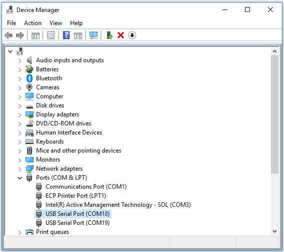
Figure 54 DA1453x/DA1458x HDK Virtual COM Port
5.5. Configuring the SWD Interface on a DA1453x/DA1458x HDK
The DA1453x/DA1458x SWD interface should be used to download the code to system RAM and debug the downloaded application.
Target chip |
SW_CLK jumper configuration |
SW_DIO jumper configuration |
|---|---|---|
DA1458x |
Connect J1.21 to J1.22 |
Connect J1.23 to J1.24 |
DA1453x |
5.6. Blinky: Your First DA1453x/DA1458x Application Example
Blinky is a simple application example that demonstrates the basic initialization of DA1453x/DA1458x with which a LED starts to blink.
The Keil project is located in the
<sdk_root_directory>\projects\target_apps\peripheral_examples\blinky.
5.6.1. Hardware Configuration
The SWD configuration described in section Section 5.5 is used to download the code to RAM.
Target chip |
jumper configuration for LED pin |
|---|---|
DA1458x |
P1_0: Connect J8.3 to J8.4 |
DA1453x |
P0_9: Connect J8.3 to J8.4 |
5.6.2. Running the Example
Once the user has built and loaded the example project to the HDK, the LED will start to blink and the following output Figure 55 from program will be visible in the console.
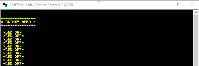
Figure 55 Blinky Demo
5.7. UART Example
The UART example demonstrates how to configure, initiate, and send-receive characters using the UART1 and UART2 ports in three different modes:
Blocking mode
Interrupt mode
DMA mode
The Keil project is located in the
<sdk_root_directory>\projects\target_apps\peripheral_examples\uart.
5.7.1. Hardware Configuration
Connect the UART terminal as described in section Section 5.4.
The SWD configuration described in section Section 5.5 is used to download the code to RAM.
The UART1/2 ports use the following HDK jumper configuration.
Target chip |
jumper configuration for UART1/2 TX pin |
jumper configuration for UART1/2 RX pin |
|---|---|---|
DA1458x |
P0_4: Connect J1.17 to J1.18 |
P0_5: Connect J1.15 to J1.16 |
DA1453x |
Connect P0_6(J2 Header) to J1.17 |
Connect P0_7(J2 Header) to J1.15 |
5.7.2. Running the Example
Once the user has built and loaded the example project to the HDK, the console will display the message shown in Figure 56, Figure 57, Figure 58, Figure 59.
The uart_print_example() function uses print_hword(), print_word() and printf_string() functions to print the message on the console.
The uart_send_blocking_example() - uart_receive_blocking_example() functions use the UART driver in blocking mode to send-receive messages.
The uart_send_interrupt_example() - uart_receive_interrupt_example() functions use the UART driver in interrupt mode to print messages on the console.
The uart_send_dma_example() - uart_receive_dma_example() functions use the UART driver in DMA mode to send-receive messages.
The last example is the uart_loopback_interrupt_example(), where every received character is echoed back to the sender.
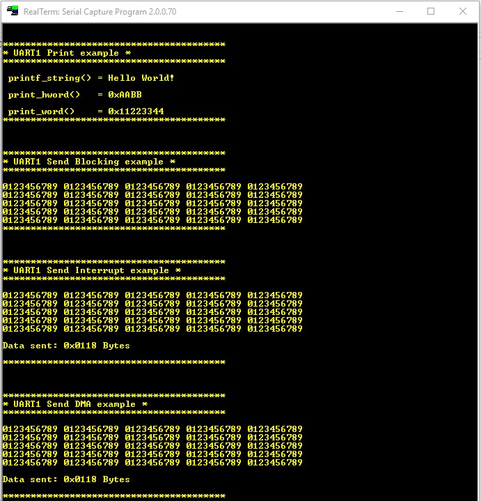
Figure 56 UART1 Send
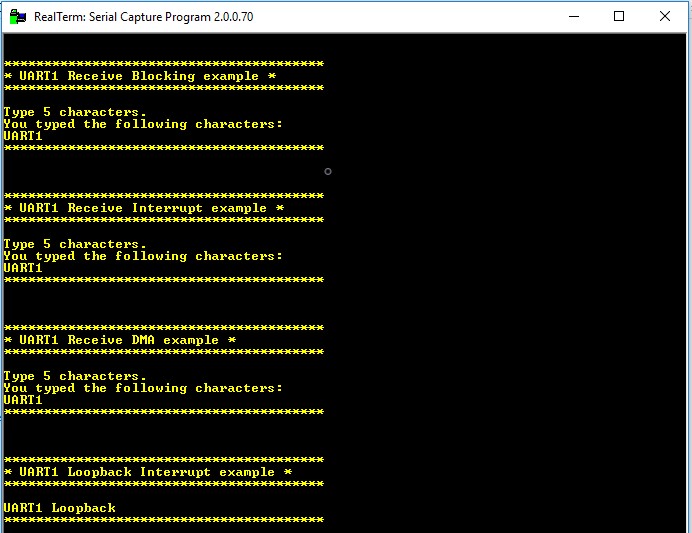
Figure 57 UART1 Receive
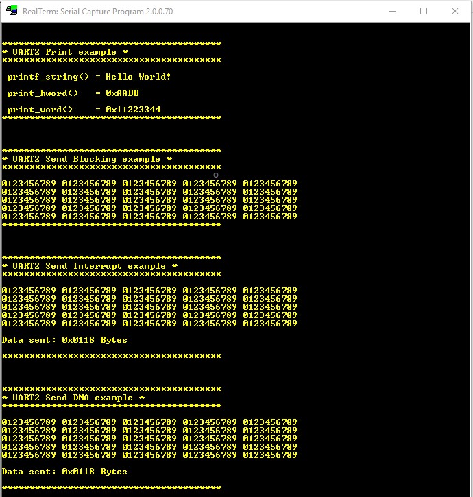
Figure 58 UART2 Send
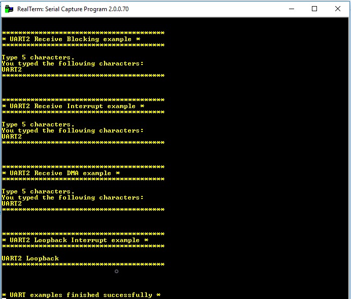
Figure 59 UART2 Receive
5.8. SPI Flash Memory Example
The SPI Flash memory example demonstrates how to initiate, read, write and erase an SPI Flash memory with the SPI Flash driver.
The Keil project is located in the
<sdk_root_directory>\projects\target_apps\peripheral_examples\spi\spi_flash.
5.8.1. Hardware Configuration
Connect the UART terminal as described in section Section 5.4.
The SWD configuration described in section Section 5.5 is used to download the code to RAM.
The SPI flash memory example uses the following HDK jumper configuration.
GPIO |
Function |
jumper configuration |
|---|---|---|
P0_0 |
SPI_CLK |
Connect J1.5 to J1.6 |
P0_3 |
SPI_CS |
Connect J1.7 to J1.8 |
P0_5 |
SPI_DI |
Connect J1.9 to J1.10 |
P0_6 |
SPI_DO |
Connect J1.3 to J1.4 |
GPIO |
Function |
jumper configuration |
|---|---|---|
P0_4 |
SPI_CLK |
Connect J1.5 to J1.6 |
P0_1 |
SPI_CS |
Connect J1.7 to J1.8 |
P0_3 |
SPI_DI |
Connect J1.9 to J1.10 |
P0_0 |
SPI_DO |
Connect J1.3 to J1.4 |
5.8.2. Running the Example
Once the user has built and loaded the example project to the HDK, a series of read and write operations will be performed on the SPI Flash memory as shown in Figure 60, Figure 61, Figure 62, Figure 63, Figure 64, Figure 65, Figure 66.
The user also has to enter the characteristics of the SPI Flash in the header
file:
<sdk_root_directory>\projects\target_apps\peripheral_examples\spi\spi_flash\include\user_periph_setup.h.
The predefined characteristics are:
#define SPI_MS_MODE             SPI_MS_MODE_MASTER
#define SPI_CP_MODE             SPI_CP_MODE_0
#define SPI_WSZ                 SPI_MODE_8BIT
#define SPI_CS                  SPI_CS_0

#define SPI_FLASH_DEV_SIZE      (256 * 1024)
The spi_test() function performs the following tests:
The GPIO pins used for the SPI Flash and the SPI module are initialized.
The SPI Flash device memory is erased. To erase a device on which protection has been activated, the full test must be run once.
The contents of the SPI Flash are read and printed to the console.
The JEDEC ID is read and the device is detected, if a corresponding entry is found in the supported device list.
The Manufacturer/Device ID and the Unique ID are read, if the device is known to be supported.
The SPI Flash device memory turned into low power mode.
The SPI Flash device memory is written with spi_flash_page_program().
The contents of the SPI Flash are read and printed to the console with spi_flash_read_data().
The SPI Flash device memory is written with spi_flash_page_program_buffer().
The contents of the SPI Flash are read and printed to the console with spi_flash_read_data_buffer().
The SPI Flash device memory is written with spi_flash_page_program_dma().
The contents of the SPI Flash are read and printed to the console with spi_flash_read_data_dma().
The SPI Flash device memory turned into high performance mode.
The SPI Flash device memory is written with spi_flash_page_program().
The contents of the SPI Flash are read and printed to the console with spi_flash_read_data().
The SPI Flash device memory is written with spi_flash_page_program_buffer().
The contents of the SPI Flash are read and printed to the console with spi_flash_read_data_buffer().
The SPI Flash device memory is written with spi_flash_page_program_dma().
The contents of the SPI Flash are read and printed to the console with spi_flash_read_data_dma().
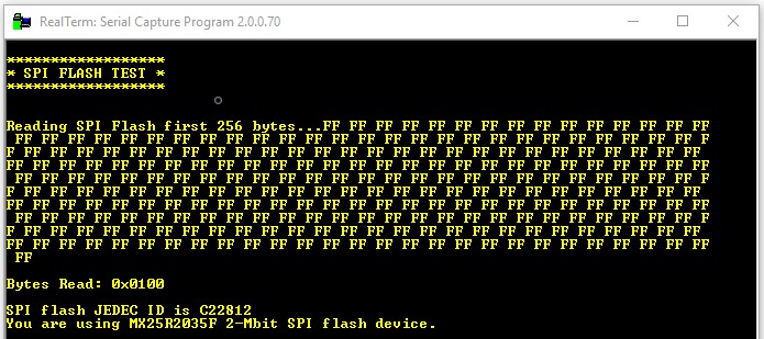
Figure 60 SPI Flash Erase

Figure 61 SPI Flash Read Write in Low Power Mode
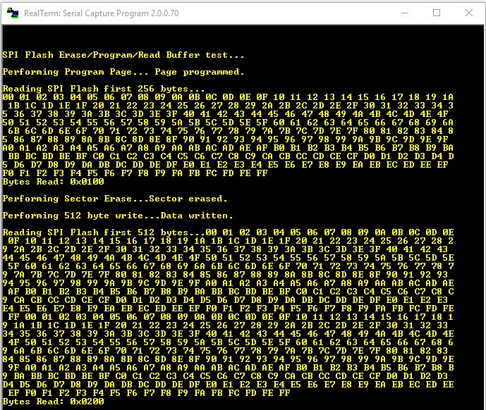
Figure 62 SPI Flash Read Write Buffer in Low Power Mode

Figure 63 SPI Flash Read Write DMA in Low Power Mode
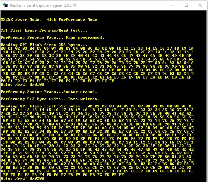
Figure 64 SPI Flash Read Write in High Performance Mode
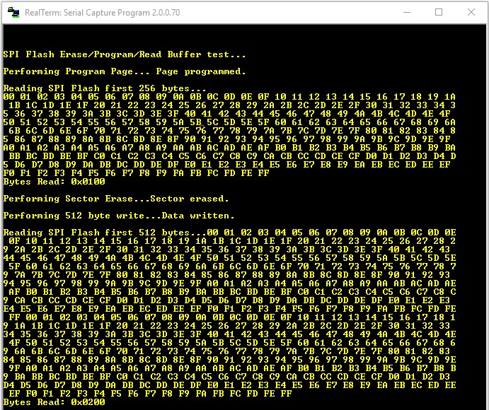
Figure 65 SPI Flash Read Write Buffer in High Performance Mode

Figure 66 SPI Flash Read Write DMA in High Performance Mode
In case you use a supported external SPI Flash device other than W25X10, the results of the SPI memory protection features test may differ. The user can change the test procedure by editing the function spi_test. The SPI Flash driver API is described in detail in API documentation.
5.9. I2C EEPROM Example
The I2C EEPROM example demonstrates how to initiate, read, write and erase an I2C EEPROM memory.
There in no I2C EEPROM chip populated on the HDK. Therefore, this example will work if the user connects an external one.
The Keil project is located in the
<sdk_root_directory>\projects\target_apps\peripheral_examples\i2c\i2c_eeprom.
5.9.1. Hardware Configuration
Connect the UART terminal as described in section Section 5.4.
The SWD configuration described in section Section 5.5 is used to download the code to RAM.
Target chip |
jumper configuration for SCL pin |
jumper configuration for SDA pin |
|---|---|---|
DA1458x |
Connect P2_3(J2 Header) to I2C EEPROM SCL |
Connect P2_1(J2 Header) to I2C EEPROM SDA |
DA1453x |
Connect P0_3(J2 Header) to I2C EEPROM SCL |
Connect P0_1(J2 Header) to I2C EEPROM SDA |
An external I2C EEPROM must be connected to the HDK using the pins shown in
Table 13.
If a different selection of GPIO pins is needed, the user should edit the
I2C_GPIO_PORT, I2C_SCL_PIN and I2C_SDA_PORT, I2C_SDA_PIN defines in
user_periph_setup.h.
5.9.2. Running the Example
Once the user has built and loaded the example project to the HDK, a series of read and writes operations will be performed on the I2C EEPROM, as shown in Figure 67, Figure 68.
The predefined I2C EEPROM characteristics are:
#define I2C_EEPROM_SIZE    0x20000              // EEPROM size in bytes
#define I2C_EEPROM_PAGE    256                  // EEPROM page size in bytes
#define I2C_SLAVE_ADDRESS  0x50                 // Set slave device address
#define I2C_SPEED_MODE     I2C_SPEED_FAST       // Speed mode: I2C_SPEED_STANDARD (100 kbits/s), I2C_SPEED_FAST (400 kbits/s)
#define I2C_ADDRESS_MODE   I2C_ADDRESSING_7B    // Addressing mode: {I2C_ADDRESSING_7B, I2C_ADDRESSING_10B}
#define I2C_ADDRESS_SIZE   I2C_2BYTES_ADDR      // Address width: {I2C_1BYTE_ADDR, I2C_2BYTES_ADDR, I2C_3BYTES_ADDR}
The i2c_test() function performs the following tests:
Initializes the GPIO pins used for the I2C EEPROM and the I2C module.
Writes 256 bytes of data to the I2C EEPROM.
Reads the contents of the I2C EEPROM.
Writes and reads bytes 0x5A, 0x6A, 0x7A and 0xFF at addresses 22, 0, 255 and 30 respectively.
Reads the contents of the I2C EEPROM.
Releases the configured GPIO pins and the I2C module.
This is shown in detail in Figure 67, Figure 68.
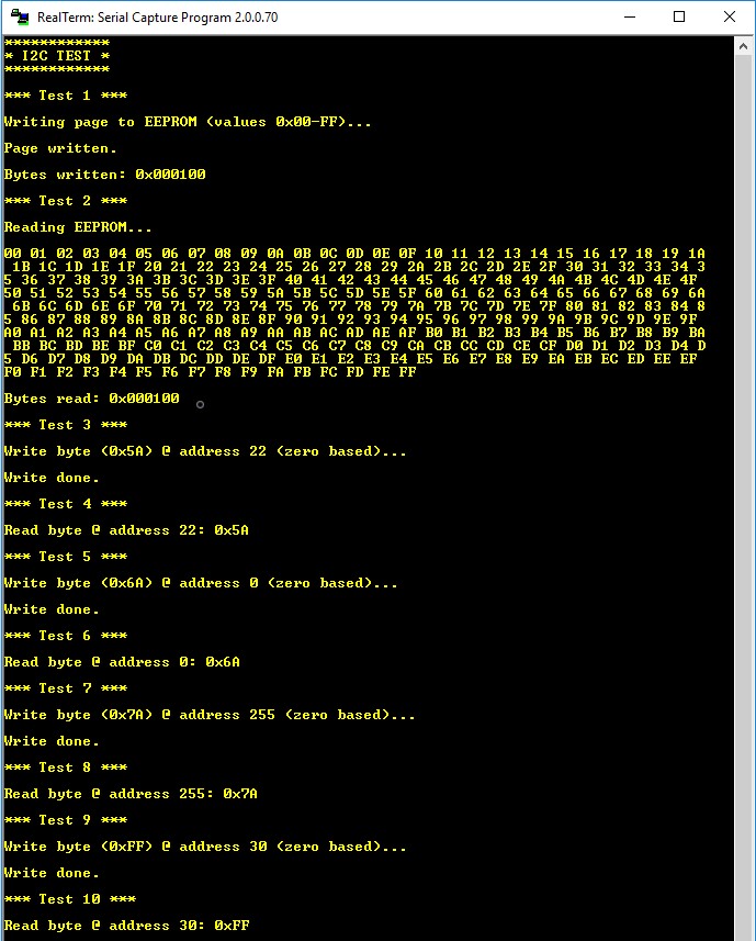
Figure 67 I2C EEPROM Read Write
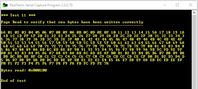
Figure 68 I2C EEPROM Verify
The user can change the test procedure by editing the function i2c_test(). The I2C EEPROM driver API is described in detail in API documentation.
5.10. Quadrature Decoder Example
The Quadrature decoder example demonstrates how to configure and read from the quadrature decoder peripheral. The Wakeup Timer setup for responding to GPIO activity is also demonstrated in this example.
There in no Quadrature encoder module populated on the HDK. Therefore, this example will work if the user connects an external one.
The Keil project is located in the
<sdk_root_directory>\projects\target_apps\peripheral_examples\quadrature_decoder.
5.10.1. Hardware Configuration
Connect the UART terminal as described in section Section 5.4.
Note
The DA1453x example uses P08 as the UART2 TX, instead of P06. The P08 pin is the J2.29 (noted as P28 in J2 connector).
The SWD configuration described in section Section 5.5 is used to download the code to RAM.
The connection settings required by the Quadrature decoder example are shown in Table 14.
Target chip |
jumper configuration for CHX_A PIN |
jumper configuration for CHX_B PIN |
jumper configuration for WKUP1 PIN |
jumper configuration for WKUP2 PIN |
|---|---|---|---|---|
DA1458x |
Connect P0_0(J2 Header) to encoder |
Connect P0_1(J2 Header) to encoder |
P0_6 :Connect J19.1 to J19.2 |
P1_1: Connect J19.4 to J19.5 |
DA1453x |
Connect P0_6(J2 Header) to encoder |
Connect P0_7(J2 Header) to encoder |
P0_11: Connect J19.1 to J19.2 |
Connect P0_1(J2 Header) to J19.4 |
The quadrature encoder CHX_A and CHX_B pins have to be connected to P0_0 and P0_1 for DA1458x and to P0_8 and P0_9 for DA1453x.
The common terminal of the quadrature encoder must be connected to ground.
The WKUP1_PIN is connected with the SW2 button on the HDK and WKUP2_PIN is connected to the SW3 button on the HDK.
5.10.2. Running the Example
Once the user has built and loaded the example project to the HDK, the console will display the screen shown in Figure 69.
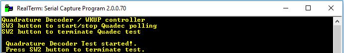
Figure 69 Quadrature Decoder Example
If the rotary encoder is activated (e.g. the mouse wheel is scrolled and the rotary encoder is attached to a mouse) the quadrature decoder-wakeup timer interrupt will be triggered, and after each trigger the terminal screen will report the axes relative coordinates. In this configuration, only the X channel terminals are configured and connected, the console will display the screen shown in Figure 70.

Figure 70 Quadrature Decoder ISR-Only Reports
If at any time the SW3 button is pressed (the user should make sure that the correct jumper configuration for buttons SW3 and SW2 is selected, as described in Section 5.10.1), polling of the relative coordinates will be enabled. Then the terminal window will start polling the quadrature decoder driver (see Figure 71). If the quadrature decoder is activated, a mixture of ISR and polling generated reports are displayed (see Figure 72).

Figure 71 Quadrature Decoder Polling-Only Reports
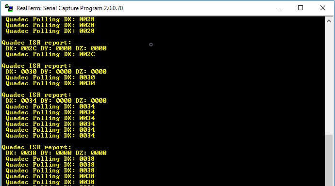
Figure 72 Quadrature Decoder Polling and ISR Reports
Click the SW3 button again to stop polling. To terminate the test, one can press SW2 at any time. The message “Quadrature Decoder Test terminated!” will be printed to the connected UART terminal.
If the count of events needs to be changed before an interrupt is triggered,
the parameter QDEC_EVENTS_COUNT_TO_INT in user_periph_setup.h can be
modified accordingly.
In the same file, one can change the clock divisor of the quadrature decoder by
altering the parameter QDEC_CLOCK_DIVIDER.
#define QDEC_CLOCK_DIVIDER                   (1)
#define QDEC_EVENTS_COUNT_TO_INT             (1)
5.11. Systick Example
The Systick example demonstrates how to use the systick timer to generate an interrupt periodically. LED is changing its state upon each interrupt.
The Keil project is located in the
<sdk_root_directory>\projects\target_apps\peripheral_examples\systick.
5.11.1. Hardware Configuration
This example does not use the UART terminal.
The debug configuration described in section Section 5.5 is used to download the code to RAM.
Target chip |
jumper configuration for LED pin |
|---|---|
DA1458x |
P1_0: Connect J8.3 to J8.4 |
DA1453x |
P0_9: Connect J8.3 to J8.4 |
5.11.2. Running the Example
Once the user has built and loaded the example project to the HDK, the LED will start to blink every 1 second.
5.12. TIMER0 (PWM0, PWM1) Example
The TIMER0 (PWM0, PWM1) example demonstrates how to configure TIMER0 to produce PWM signals. A melody is produced on an externally connected buzzer.
The Keil project is located in the
<sdk_root_directory>\projects\target_apps\peripheral_examples\timer0\timer0_pwm.
5.12.1. Hardware Configuration
Connect the UART terminal as described in section Section 5.4.
The SWD configuration described in section Section 5.5 is used to download the code to RAM.
Target chip |
jumper configuration for PWM0 pin |
jumper configuration for PWM1 pin |
|---|---|---|
DA1458x |
Connect buzzer between P0_2(J2 Header) and Ground |
Connect buzzer between P0_3(J2 Header) and Ground |
DA1453x |
Connect buzzer between P0_9(J2 Header) and Ground |
Connect buzzer between P0_8(J2 Header) and Ground |
5.12.2. Running the Example
Once the user has built and loaded the example project to the HDK, the PWM0 and PWM1 signals will become active and start producing an audible melody if a buzzer is connected to P0_2 - P0_3 for DA1458x targets or P0_9 - P0_8 for DA1453x target. While the melody is playing, stars are being drawn in the terminal window on each beat Figure 73.
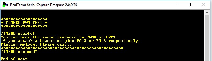
Figure 73 Timer0 PWM
5.13. TIMER0 General Example
The TIMER0 general example demonstrates how to configure TIMER0 to count a specified amount of time and generate an interrupt. A LED is changing state upon each timer interrupt.
The Keil project is located in the
<sdk_root_directory>\projects\target_apps\peripheral_examples\timer0\timer0_general.
5.13.1. Hardware Configuration
Connect the UART terminal as described in section Section 5.4.
Target chip |
jumper configuration for LED pin |
|---|---|
DA1458x |
P1_0: Connect J8.3 to J8.4 |
DA1453x |
P0_9: Connect J8.3 to J8.4 |
5.13.2. Running the Example
Once the user has built and loaded the example project to the HDK, the LED will be changing its state every second until the end of the test. The duration of the test (expressed in seconds) can be set by user and it will also be printed in the console. See Figure 74.

Figure 74 Timer0 General
5.14. TIMER2 (PWM2, PWM3, PWM4) Example
The TIMER2 (PWM2, PWM3, PWM4) example demonstrates how to configure TIMER2 to produce PWM signals. The PWM outputs are used to change the brightness of the LEDs in this example.
The Keil project is located in the
<sdk_root_directory>\projects\target_apps\peripheral_examples\timer2\timer2_pwm.
5.14.1. Hardware Configuration
Connect the UART terminal as described in section Section 5.4.
The SWD configuration described in section Section 5.5 is used to download the code to RAM.
Target chip |
jumper configuration for PWM2 pin |
jumper configuration for PWM3 pin |
jumper configuration for PWM4 pin |
|---|---|---|---|
DA1458x |
P1_2(J2 Header) |
P0_7(J2 Header) |
P1_0(J2 Header) |
DA1453x |
P0_8(J2 Header) |
P0_9(J2 Header) |
P0_7(J2 Header) |
The user can use LED segment array as a visual indication for signals PWM2, PWM3 and PWM4. The brightness of the LED segments is then directly influenced by the duty cycle of the PWM signals.
5.14.2. Running the Example
Once the user has built the Timer2 (PWM2, PWM3, PWM4) example and loaded to HDK, the PWM2, PWM3 and PWM4 signals will become active. If a LED segment array is connected to the PWM pins. The brightness of the LEDs will be changing automatically because each PWM duty cycle will change in a loop function. The screen shown in Figure 75 will appear.

Figure 75 Timer2 PWM
5.15. Battery Example
The Battery example demonstrates how to read the battery level with the use of the ADC.
The Keil project is located in the
<sdk_root_directory>\projects\target_apps\peripheral_examples\adc\batt_lvl.
5.15.1. Hardware Configuration
Connect the UART terminal as described in section Section 5.4.
The SWD configuration described in section Section 5.5 is used to download the code to RAM.
The user has to install a coin cell battery on the board.
5.15.2. Running the Example
Once the user has built and loaded the example project to the HDK, the ADC is configured to provide a measurement of the battery level. If device operates in boost mode, the example will report the percentage left of an alkaline cell battery on the terminal screen (see Figure 76) – if not, the percentage left of a CR2032 cell battery will be reported instead (see Figure 77).

Figure 76 Battery Example – Boost Mode
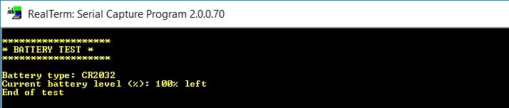
Figure 77 Battery Example