3. Analyzing The Demonstration Example
This section analyzes an application example which demonstrates using the SPI adapters. The example is based on the freertos_retarget sample code found in the SDK. It adds two additional freeRTOS tasks which are responsible for various SPI operations. One task performs loopback tests using the SPI1 interface in duplex mode, while the second task controls an external SPI module, connected on SPI1 bus. The code also enables the Wake-up timer for handling external events. Both synchronous and asynchronous SPI operations are demonstrated.
3.1. Application Structure
- The key goal of this demonstration is for the device to perform a few SPI operations following an event.
For demonstration purposes the K1 button on the Pro DevKit has been configured as a wake-up input pin. For more information
on how to configure and set a pin for handling external events, please read the External Interruption
tutorial. At each external event (produced at every button press - K1 on Pro Devkit) a dedicated
callback function named
wkup_cb()is triggered.

Fig. 9 Echo Task - Main Execution Path
In this function, the task responsible for the SPI loopback tests is signaled so that it can unblock. In this freeRTOS task, a duplex transaction takes place, that is, the data shifted out from the MOSI pin is shifted in from the MISO pin at the same time. Upon finishing the transaction, a data integrity check is performed and the corresponding debugging message is printed out on the serial console.
- At the same time, at every 100 ms time interval, the task which is responsible for controlling the
MCP4822 DAC module is executed. Depending on the value of the
SPI_ASYNC_ENmacro, a synchronous or an asynchronous SPI write operation is performed. A 2-byte data is sent over the SPI bus to update the analog output value of the MCP4822 DAC module. A variable nameddataholds both the control bits as well as the raw data. At the end of every SPI transaction, the raw data increments thus increasing the output analog value of the DAC module.
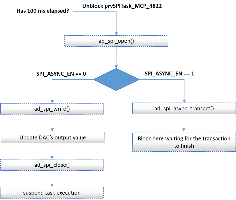
Fig. 10 MCP4822 Write SW FSM - Main Execution Path
- As mentioned, the
SPI_ASYNC_ENmacro can be used to enable asynchronous SPI write operations. To do this, set the macro to'1'. As described in SPI Transactions, developers must not call asynchronous related APIs without guaranteeing that the previous asynchronous transaction is finished. To ensure this, after calling thead_spi_async_transact()function, the code waits for the arrival of a signal, indicating the end of the current SPI operation.
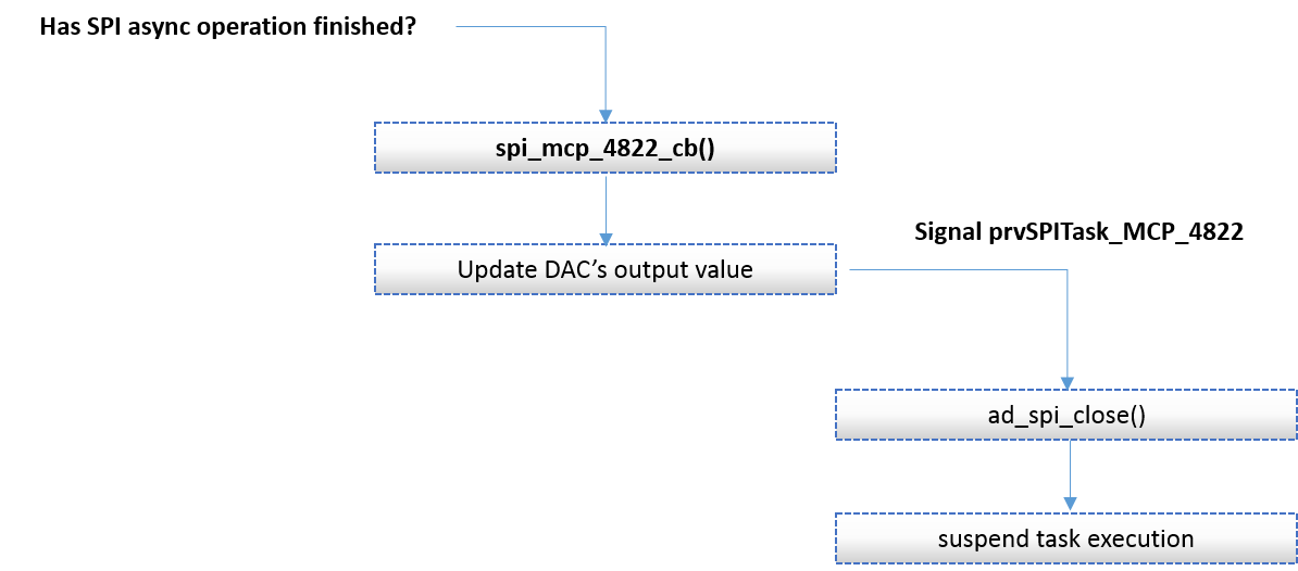
Fig. 11 MCP4822 Async Write SW FSM - Callback Function Execution Path
- The selected DAC module consists of a 2-byte register,
in which the first four significant bits (MSBits) control the entire behavior of the module. Since the
demonstrated example masks all four configuration bits with 0xF000, it is expected that
the module is in active mode and VoutB is activated. For more information on the control bits, read the
Serial Interfacesection in the manufacturer datasheet.
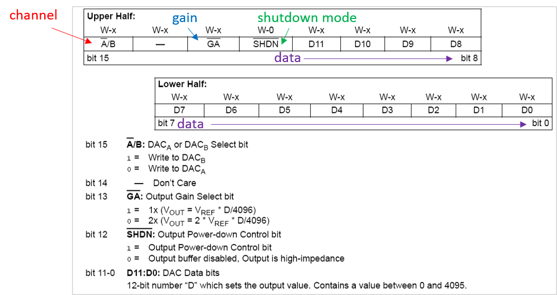
Fig. 12 Control & Data bits of MCP4822 DAC Chip
Note
The MCP4822 DAC module has been selected for demonstration purposes only. Providing complete drivers for this module is out of the scope of this tutorial.