2. Power Consumption
2.1. Factors influencing the power consumption
There are numerous parameter affecting the power consumption of such a complex system even when executing what appears as the same application scenario. Thus before presenting numbers and results we will focus on the basic parameters and configuration options of DA1470x that influence the power consumption and how.
2.2. Power generation
The following diagram presents a simplified view of the power management unit of the system in a typical usecase.
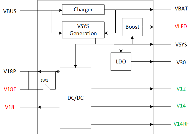
Power requirements are a concern when using a battery. When the device is being charged the assumption is that power is no longer a critical parameter and therefore the device is kept awake.
As shown in the diagram the Battery will provide power to VSYS. In practice VSYS is sorted with VBAT through a switch. From VSYS rail in the typical usecase we will generate all other rail voltages either using DC/DCs or LDOs. The following table shows the way the different rail voltages are generated.
Rail |
Source |
Generator Type |
Use |
|---|---|---|---|
VSYS |
VBAT |
Switch |
Power to the rest of the system |
V30 |
VSYS |
LDO |
Power to internal modules of DA1470x |
V12 |
VSYS |
DC/DC |
Power the digital core of DA1470x |
V14/V14RF |
VSYS |
DC/DC |
Power the radio of DA1470x |
V18 |
VSYS |
DC/DC |
Power external components |
V18F |
V18P |
SW1 - External short |
Power external OSPI/QSPI flash |
V18P |
VSYS |
DC/DC |
Power GPIOs, VAD or external components. |
Some of the rails are used to power internal components of the system and other rails are intented to power external components. A point to highlight here is that V18P and V18F may be externally shorted due to the resistance of SW1 which may produce significant drop in the case of high powered OSPI/QSPI flashes.
2.3. Power domains
The figure below gives an overview of the different power domains of DA1470x.
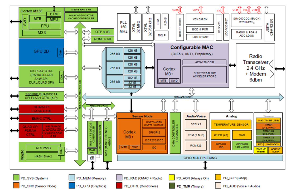
Table 2 summarizes the logic powered from each domain. Needless to say that each power domain will contribute on the overall power consumption. Depending on the configuration (clocks configuration, voltage setting) and the logic exercised during a test a different power consumption datapoint will be generated.
Name |
Description |
Contains |
|---|---|---|
PD_SYS |
System power domain |
Arm Cortex M33, Cache Controller, Octa/Quad SPI controller (XiP), OTP Controller, ROM, Crypto Block, USB Controller, Charge Detection, Charger FSM, SPI3, DMA controller, APP ADC, Display Controller (Parallel/JDI, 3/4w SPI, Dual/Quad SPI), AMBA AHB, APB-32 fast |
PD_MEM |
Memory power domain |
Memory Controller, XTAL32M FSM, PLL160M regs,PLL48M regs, GPIO multiplexing, APB-32 slow, Clock calibration |
PD_RAD |
Radio power domain CMAC |
Modem, RFMON, RFCU |
PD_AON |
Always On power domain |
Wake up from Hibernation controller |
PD_SLP |
Sleep power domain MAC Timer |
RTC, System Watchdog, Wake up from Sleep controller, Buck DCDC FSM, Boost DCDC FSM, WLEDs, VAD digital FSM, clock-tree |
PD_SNC |
Sensor Node Controller power domain |
SNC Cortex M0+, all serial interfaces (except SPI3), GP ADC |
PD_GPU |
GPU power domain |
2D GPU |
PD_CTRL |
External Memory Controller power domain |
Quad SPI controllers for flash and PSRAM, write-back cache controller, and eMMC host controller |
PD_AUD |
Audio power domain |
Audio/Voice interface controllers |
PD_TMR |
Timers power domain |
Timer, Timer2, Timer3, Timer4, Timer5, Timer6 |
2.4. Power Modes
The power modes are closely related to possible application states. Table 3 summarizes the possible options of the available clocks, the power generation configuration and power domain state for each power mode. Looking in the data of the table one can see that there are very large number of different configuration for each power mode and providing a single number is not practical or representative of a power mode.
Power Mode |
Power Domains |
LDOs and DCDC Converters |
Clocks available |
Real-Time Clock |
Wake-Up from |
Active |
PD_SYS=Optional PD_SNC=Optional PD_MEM=Active PD_GPU=Optional PD_RAD=Optional PD_CTRL=Optional PD_AON=Active PD_TMR=Optional PD_SLP=Active PD_AUD=Optional |
VSYS Generation = ON LDO_V30 = ON, LDO_V30_RET = OFF LDO_START = OFF V30 CLAMP = OFF, VDD clamp ON BUCK = ON BOOST = OPTIONAL |
All |
Running |
N/A |
VAD Sleep |
PD_SYS=OFF PD_SNC=OFF PD_MEM=OFF PD_GPU=OFF PD_RAD=OFF PD_CTRL=OFF PD_AON=ON PD_TMR=Optional PD_SLP=ON PD_AUD=OFF |
VSYS Generation = ON LDO_V30 = OPTIONAL, LDO_V30_RET = ON LDO_START = OFF V30 CLAMP = OFF, VDD clamp ON BUCK = low IQ mode BOOST = OPTIONAL |
RCX RCLP XTAL32K |
Running |
VAD interrupt GPIO Toggle RTC Alarm Timer Expiration MAC Timer Expiration VBUS Available nRST pin |
Extended Sleep |
PD_SYS=OFF PD_SNC=OFF PD_MEM=OFF PD_GPU=OFF PD_RAD=OFF PD_CTRL=OFF PD_AON=ON PD_TMR=Optional PD_SLP=ON PD_AUD=OFF |
VSYS Generation = ON LDO_V30 = OPTIONAL, LDO_V30_RET = ON LDO_START = OFF V30 CLAMP = OFF, VDD clamp ON BUCK = ON BOOST = OPTIONAL |
RCX RCLP XTAL32K |
Running |
GPIO Toggle RTC Alarm Timer Expiration MAC Timer Expiration VBUS Available nRST pin |
Deep Sleep |
PD_SYS=OFF PD_SNC=OFF PD_MEM=OFF PD_GPU=OFF PD_RAD=OFF PD_CTRL=OFF PD_AON=ON PD_TMR=Optional PD_SLP=ON PD_AUD=OFF |
VSYS Generation = ON LDO_V30 = OPTIONAL, LDO_V30_RET = ON LDO_START = OFF V30 CLAMP = OFF, VDD clamp ON BUCK = ON BOOST = OFF |
RCX RCLP XTAL32K |
Running |
GPIO Toggle RTC Alarm Timer Expiration MAC Timer VBUS Available nRST pin |
Hibernation |
PD_SYS=OFF PD_SNC=OFF PD_MEM=OFF PD_GPU=OFF PD_RAD=OFF PD_CTRL=OFF PD_AON=ON PD_TMR=OFF PD_SLP=OFF PD_AUD=OFF |
VSYS Generation = OFF LDO_V30 = OFF, LDO_V30_RET = OFF LDO_START = OFF V30 CLAMP = OFF VDD clamp ON BUCK = OFF BOOST = OFF |
None |
No RTC |
GPIO Toggle VBUS Available |
2.5. Other factors influencing the power consumption
2.5.1. Clock
Clock selection will always influence power consumption measurements. Faster clocks as expected will increase power consumption. Oscillators will add in the power budget compared to an RC clock of the same frequency due to the additional power consumption of the oscillator. We need not to forget also the numerous clock divisors that exist in the system, with the hclk and pclk of the AMBA bus making the most difference on the power consumption results on a test scenario.
2.5.2. Code execution on different processors (CMAC, M33, M0)
DA1470x integrates 3 ARM cores. A different power consumption profile is expected when executing even the same piece of code in the application processor M33 and the SNC (M0) with the later expected to consume less power. In the case of the application processor (M33) the memory from which the code is fetched will greatly influence the power consumed. Whether it is the OSPI/QSPI flash through the i-cache at a specific cache miss ratio, a fully cached piece of code or an internal RAM block different numbers are expected for even apparently the same application code.
Summarizing:
the power domains enabled,
the clock configuration,
the rails enabled and
the external loads hooked
on them, the MCU used and the memory used to read the code will all influence a power measurement of a device under a specific test.