4. Middleware
4.1. System
4.1.1. Power and Clock Management
4.1.1.1. Introduction
This section illustrates :
The basic steps of the system when it goes to sleep and when it wakes up.
The supported power modes.
The basic system calls needed by the application to initialize the clock and the power management.
4.1.1.2. Going to sleep and waking up steps
The basic walk through is shown in Figure 11.

Figure 11 Going to sleep and waking up steps
Note
In case of different paths, the color of the arrow matches with the color of the comment.
4.1.1.3. Supported power modes
The supported power modes are depicted in Table 16.
Power mode |
Description |
|---|---|
active |
|
idle |
|
extended sleep |
|
deep sleep |
|
hibernation |
|
4.1.1.4. Initializing clock and power management
The flow for an application to initialize the clock and the power management is shown in Figure 13.

Figure 13 Power and clock manager initialization
4.1.2. Watchdog Service
4.1.2.6. Description
The system watchdog service (sys_watchdog) has been designed to monitor
system tasks and avoid system freezes. The interaction of this service
with other parts of the system is shown in Figure 15:

Figure 15 Watchdog overview
Effectively, sys_watchdog is a layer on top of the watchdog low-level driver that allows multiple tasks to share the underlying hardware watchdog timer. The watchdog service can be used to trigger a full system reset. This will allow system to recover from a catastrophic failure in one or more tasks.
4.1.2.7. Concept
A task that should be monitored has to first register itself with this
service to receive a unique handle (id). The task must then is
periodically notify sys_watchdog using this id, to signal that the task
working properly. In case of any error during registration, the invalid id
-1 is returned.
The hardware watchdog is essentially a countdown timer, which is powered by the always on domain (PD_AON) and it will be automatically enabled as soon as the system powers up. It is decremented by 1 every ~10 ms (assuming default source clock the RC32K) and it is set to max value at reset. This results to a maximum watchdog time-out of 84 seconds. If the RCX is used as a source clock, the time-out time is even longer, depending on the RCX frequency.
If WATCHDOG_CTRL_REG[NMI_RST] = 0, the watchdog timer will generate an
NMI to the Cortex M33 when the watchdog timer reaches 0 and a HW reset
when the counter becomes less or equal to -16. The NMI handler must write
any value > -16 to the WATCHDOG_REG to prevent the generation of a
WDOG reset within 16x10 = 160 ms. If WATCHDOG_CTRL_REG[NMI_RST] = 1, the
watchdog timer generates a WDOG reset if the timer becomes less than or equal
to 0.
To prevent this, the watchdog timer must be reset to its starting value before
it expires. This starting value can be configured in the application custom
configuration files via the numerical macro dg_configWDOG_RESET_VALUE. Its
default value is the maximum 0xFF, which corresponds to approximately 2.6
seconds (assuming default source clock the RC32K). The maximum number of tasks
that can be monitored is defined by the configuration macro
dg_configWDOG_MAX_TASKS_CNT. Its default value is 6 (the absolute maximum
is 32).
If during one watchdog period all monitored tasks notify sys_watchdog,
the hardware watchdog will be updated via the
hw_watchdog_set_pos_val() LLD API function; in this case, no
platform reset will be triggered for this watchdog period. However, a
platform reset will be triggered if at least one task does not notify
sys_watchdog in time. There are two ways for a task to notify
sys_watchdog.
Each task is responsible for periodically notifying sys_watchdog that it is
still running using sys_watchdog_notify(). This must be done before the watchdog
timer expires. Occasionally a registered task may want to temporarily exclude itself
from being monitored if it expects to be blocked for a long time waiting for an event.
This is done using the sys_watchdog_suspend() API function. This function suspends
monitoring of specific tasks in sys_watchdog, as there is no need to monitor a task
that is blocked waiting for an event that might take too long to occur (i.e. it would
lead to the task failing to notify the watchdog service, thus resulting in a system reset).
When the task is unblocked, the sys_watchdog_resume() API function should be
called to restore task monitoring by the watchdog service. From that moment on the
task shall notify the watchdog service as usual.
Finally, the sys_watchdog_set_latency() API function is intended to
be used in cases where a task would require a watchdog period greater
than the configured watchdog timer reset value. Using this API allows a
task to delay notification of sys_watchdog for a given number of
watchdog periods, without triggering a system reset. The effect of
calling the API function is one-off, thus it must be set every time
increased latency is required.
4.1.2.8. Examples
To register the task with sys_watchdog use the following code snippet
/* register pxp task to be monitored by watchdog */
wdog_id = sys_watchdog_register(false);
To notify sys_watchdog use sys_watchdog_notify(). If the task is going to suspend for an event then temporarily exclude the current task from being monitored using sys_watchdog_suspend(). Once the task has received an event it can resume its watchdog operation with sys_watchdog_resume(). This flow is shown below :
/*
* notify watchdog on each loop since there's no other trigger for this - monitoring
* will be suspended while blocking on OS_TASK_NOTIFY_WAIT()
*/
sys_watchdog_notify(wdog_id);
/*
* Wait on any of the event group bits, then clear them all
*/
sys_watchdog_suspend(wdog_id);
ret = OS_TASK_NOTIFY_WAIT(0, OS_TASK_NOTIFY_ALL_BITS, ¬if, OS_TASK_NOTIFY_FOREVER);
/*
* Blocks forever waiting for the task notification. Therefore, the return value must
* always be OS_OK
*/
OS_ASSERT(ret == OS_OK);
sys_watchdog_resume(wdog_id);
4.1.2.8.1. API
Function |
Description |
|---|---|
void sys_watchdog_init (void) |
Initialize This should be called before using the |
int8_t sys_watchdog_register(bool notify_trigger) |
Register current task with the |
void sys_watchdog_unregister(int8_t id) |
Unregister task from the |
void sys_watchdog_configure_idle_id(int8_t id) |
Inform |
void sys_watchdog_suspend(int8_t id) |
Suspend task being monitoring by the A monitor-suspended task is not unregistered entirely, but it is ignored by the watchdog service until its monitoring is resumed. It is faster than unregistering and registering the task again. |
void sys_watchdog_resume(int8_t id) |
Resume monitoring of a task by the It should be called as soon as the reason that |
void sys_watchdog_notify(int8_t id) |
Notify A registered task shall call this API function periodically to notify |
void sys_watchdog_notify_and_resume(int8_t id) |
Notify This function combines the functionality of |
void sys_watchdog_set_latency(uint8_t id, uint8_t latency) |
Set watchdog latency for a task. This allows a task to miss a given number of notification periods to |
4.1.3. The Charger
4.1.3.1. Introduction
This section describes the DA1469x charger software implementation and its integration in the SmartSnippets™ DA1469x SDK. It describes also the System’s charging operation and how to use System’s charging service.
USB Connection Terminology
Attach: A downstream device is considered to be attached to an upstream port when there is a physical cable between the two.
Connect: A downstream device is considered to be connected to an upstream port when it is attached to the upstream port, and when the downstream device has pulled either the D+ or D- data line high through a 1.5 kΩ resistor, in order to enter Low-Speed, Full-Speed or High-Speed signalling.
Enumerate: The initial data exchange between a PD and the host to identify the device type.
Port description
Port description can be retrieved from [Ref_03].
4.1.3.2. Software architecture
The charger’s code is executed by the Cortex M33. It needs to support the charging procedure of Li-On rechargeable batteries.

Figure 16 Charger’s layers
Charger’s layers are depicted in Figure 16. In more detail:
- Hardware which consists of:
HW FSM (including the main FSM and JEITA FSM)
Data Contact Detection (DCD) and Port Detection
VBUS Detection
Low Level Driver (LLD), an abstraction layer consisting of services accessing the HW resources.
Middleware a secondary abstraction layer which “glues” the LLD services and forwards the registered events to the application.
4.1.3.3. Low Level Driver
The conceptual entity organisation of the charger’s LLD is described in Figure 17.
Figure 17 Entity associations of the charger’s LLD
The upper layer programs/sets up the HW FSM by defining:
A charging profile
The fine tuning settings (if there is a need to overwrite the default values)
The IRQ callback functions for retrieving state/transition and error events out of the HW FSM

Figure 19 Flowchart of the charger’s LLD
The corresponding procedures taking place during HW FSM configuration are shown in Figure 19, while Figure 20 depicts the actual states of the HW FSM.

Figure 20 Charger’s HW FSM
4.1.3.4. Middleware
The basic steps the middleware goes through are shown in Figure 21.

Figure 21 Middleware high level flowchart
The steps are the following:
Detect that a USB cable has been physically connected.
Start the port detection procedure in order to determine the current budget provided by the host side.
Program the HW FSM according to the battery specification.
Send notifications to the application.
Detect that the USB cable has been physically disconnected.
4.1.3.5. System charging operation
The internals of the charger’s middleware layer and how the notifications are forwarded to the application are depicted in more detail in Figure 22.

Figure 22 System charger operation
The next image Figure 25 shows the flow chart of the USB port detection. The type of the port influences the maximum current budget the charger can draw.

Figure 25 USB charging port detection
4.1.3.6. Using the system charging service
The charging system service is a daemon that:
Detects the VBUS presence.
Runs the port detection algorithm.
Programs the HW FSM according to the application charging profile taking into account the port detection result.
Notifies the application for the events the latter is interested in.
Note
The charging daemon depends on the Operating System services.
4.1.3.7. Configuring the system charging service
The following need to be configured for employing the charging service:
Enable the charging service configuration option
In the custom header file (for example, custom_config_qspi.h) the next entry needs to be enabled.
#define dg_configUSE_SYS_CHARGER 1
In the source code USB data pins must be configured accordingly:
/* USB data pin configuration */
hw_gpio_set_pin_function(HW_GPIO_PORT_0, HW_GPIO_PIN_14, HW_GPIO_MODE_INPUT, HW_GPIO_FUNC_USB);
hw_gpio_set_pin_function(HW_GPIO_PORT_0, HW_GPIO_PIN_15, HW_GPIO_MODE_INPUT, HW_GPIO_FUNC_USB);
This usually takes place in the void periph_init() function.
If the battery temperature needs to be monitored, the NTC pins must be configured accordingly:
 /* Pin configuration for the NTC */
/* Pin configuration for the NTC */
 hw_gpio_set_pin_function(HW_GPIO_PORT_0, HW_GPIO_PIN_7, HW_GPIO_MODE_INPUT, HW_GPIO_FUNC_GPIO);
 hw_gpio_set_pin_function(HW_GPIO_PORT_1, HW_GPIO_PIN_0, HW_GPIO_MODE_OUTPUT, HW_GPIO_FUNC_GPIO);

 hw_gpio_set_active(HW_GPIO_PORT_1, HW_GPIO_PIN_0);

 hw_gpio_pad_latch_enable((HW_GPIO_PORT_1), (HW_GPIO_PIN_0));
 hw_gpio_pad_latch_disable((HW_GPIO_PORT_1), (HW_GPIO_PIN_0));
This usually takes place in the void periph_init() function.
Add a custom charging profile, for example:
static const sys_charger_configuration_t sys_charger_conf = {
      {
            .ctrl_flags = HW_CHARGER_CTRL_ENABLE_DIE_TEMP_PROTECTION                        |
                           HW_CHARGER_CTRL_RESUME_FROM_DIE_PROTECTION_STATE                  |
                           HW_CHARGER_CTRL_ENABLE_BAT_TEMP_PROTECTION                        |
                           HW_CHARGER_CTRL_ENABLE_JEITA_SUPPORT                              |
                           HW_CHARGER_CTRL_RESUME_FROM_ERROR_STATE                           |
                           HW_CHARGER_CTRL_HALT_CHARGE_TIMERS_ON_TEMP_PROTECTION_STATES,

            /* Tbat monitoring settings */
            .tbat_monitor_mode = HW_CHARGER_TBAT_MONITOR_MODE_PERIODIC_FSM_ON,

            /* IRQ settings */
            .irq_ok_mask = HW_CHARGER_FSM_IRQ_OK_ALL ^
                           (HW_CHARGER_FSM_IRQ_OK_MASK(TBAT_STATUS_UPDATE)  |
                            HW_CHARGER_FSM_IRQ_OK_MASK(CV_TO_CC)            |
                            HW_CHARGER_FSM_IRQ_OK_MASK(CC_TO_CV)),
            .irq_nok_mask = HW_CHARGER_FSM_IRQ_NOK_ALL,

            /* Voltage settings */
            .ovp_level = HW_CHARGER_V_LEVEL_4900,
            .replenish_v_level = HW_CHARGER_V_LEVEL_4000,
            .precharged_v_thr = HW_CHARGER_V_LEVEL_3000,
            .cv_level = HW_CHARGER_V_LEVEL_4200,

            /* Current settings */
            .eoc_i_thr = HW_CHARGER_I_EOC_PERCENT_LEVEL_10,
            .precharge_cc_level = HW_CHARGER_I_PRECHARGE_LEVEL_10,
            .cc_level = HW_CHARGER_I_LEVEL_120,

            /* Default JEITA voltage settings */
            .jeita_ovp_cool_level = HW_CHARGER_V_LEVEL_4480,
            .jeita_ovp_warm_level = HW_CHARGER_V_LEVEL_4460,
            .jeita_replenish_v_cool_level = HW_CHARGER_V_LEVEL_4020,
            .jeita_replenish_v_warm_level = HW_CHARGER_V_LEVEL_4000,
            .jeita_precharged_v_cool_thr = HW_CHARGER_V_LEVEL_3150,
            .jeita_precharged_v_warm_thr = HW_CHARGER_V_LEVEL_3100,
            .jeita_cv_cool_level = HW_CHARGER_V_LEVEL_4200,
            .jeita_cv_warm_level = HW_CHARGER_V_LEVEL_4220,

            /* Default JEITA current settings */
            .jeita_precharge_cc_cool_level = HW_CHARGER_I_PRECHARGE_LEVEL_1_5,
            .jeita_precharge_cc_warm_level = HW_CHARGER_I_PRECHARGE_LEVEL_1_0,
            .jeita_cc_cool_level = HW_CHARGER_I_LEVEL_30,
            .jeita_cc_warm_level = HW_CHARGER_I_LEVEL_25,

            /* Default Tbat limits */
            .bat_temp_cold_limit = HW_CHARGER_BAT_TEMP_LIMIT_0,
            .bat_temp_cool_limit = HW_CHARGER_BAT_TEMP_LIMIT_10,
            .bat_temp_warm_limit = HW_CHARGER_BAT_TEMP_LIMIT_35,
            .bat_temp_hot_limit =  HW_CHARGER_BAT_TEMP_LIMIT_45,

            /* Tdie settings */
            .die_temp_limit = HW_CHARGER_DIE_TEMP_LIMIT_90,

            /* Default charging timeout settings */
            .max_precharge_timeout = 0x708,         /*  30min */
            .max_cc_charge_timeout = 0x1C20,        /* 120min */
            .max_cv_charge_timeout = 0x1C20,        /* 120min */
            .max_total_charge_timeout = 0x3F48      /* 270min */
      }
   };
The corresponding fields of a charging profile are documented in [Ref_04]. Variable sys_charger_conf can be declared on a separate file to ease project segregation and is an optional step. If this approach is to be followed, then the compiler’s include-directories could need an update.
Call
sys_usb_init(),sys_charger_init()insidesystem_init()task. For example:
static void system_init( void *pvParameters )
{
       /* … */
       /* Initialize USB service */
       sys_usb_init();
       /* Initialize charging service */
       sys_charger_init(&sys_charger_conf);
       /* … */
       /* Initialize BLE Manager */
       ble_mgr_init();
       /* … */
}
4.1.3.8. Notifications
The notification hook functions can be found in <SDK_ROOT_PATH>/sdk/bsp/system/sys_man/include/sys_charger_v2.h and are documented in [Ref_04].
4.1.3.10. Supported battery types
Battery types |
Description |
|---|---|
LiCoO2 |
Lithium cobalt oxide |
LiMn2O4 |
Lithium ion manganese oxide |
LiFePO4 |
Lithium iron phosphate |
LiNiCoAlO2 |
Lithium Nickel Cobalt Aluminum Oxide |
4.1.4. ADC Service
4.1.4.1. Description
The system ADC service (sys_adc) has been designed to monitor periodically the on-chip temperature
using Sensor Node Controller (SNC) and notify the application in case the temperature exceeds the specified limits.
The interaction of this service with other parts of the system is shown in Figure 26:

Figure 26 ADC service overview
4.1.4.2. Concept
The sys_adc registers an SNC ucode with a custom callback and also configures and starts the RTC. The registered ucode
executes periodically on an RTC-to-PDC event to monitor the temperature. Upon every RTC event, whose period is defined through
RTC_PDC_EVENT_PERIOD_REG register, and if the current temperature is less than the lower or greater than the upper limit,
the ucode notifies CM33.
In order for an application to utilize the sys_adc to monitor the on-chip temperature, a GPADC service must be configured using
the sys_adc_config(). The function takes as input parameters the desirable temperature offset in order for the lower and upper limits
to be determined accordingly, the period of the RTC-to-PDC event and a custom callback, which is called upon SNC ucode notification.
Using the API the application is capable of enabling/disabling the monitoring, setting different temperature offset and getting
the value for which CM33 was notified.
An example of using sys_adc service is located in the projects/dk_apps/demos/snc_gpadc_demo folder.
4.1.4.3. System use
The SmartSnippets™ DA1469X SDK enables and internally uses the service by default, in all the configurations requiring temperature monitoring, namely:
BLE applications (for triggering RF calibration)
Applications using RCX (for triggering clock calibration)
When sys_adc is used by the system (cases above) the period of RTC-to-PDC event is configured using dg_configRTC_PDC_EVENT_PERIOD and set by default to 1 second.
The application can still make use of sys_adc (in parallel to the system use), with the limitation that the period of RTC-to-PDC event is fixed to dg_configRTC_PDC_EVENT_PERIOD.
#define dg_configRTC_PDC_EVENT_PERIOD (100) // in 10ms
Note
The period for the RF calibration SNC ucode is inextricably linked to the above macro. For details on how to set the specific value see the SmartSnippets™ DA1469X SDK Documentation.
4.1.4.4. Audio Manager
4.1.4.4.1. Introduction
Audio manager is a middleware component for configuring the APU (Audio Processing Unit). It provides an API for easily setting up audio paths.
4.1.4.4.2. Software architecture
Figure 30 Audio Framework Architecture
As shown in the Audio Framework Architecture in Figure 30, the Audio Manager:
Provides an api for configuring, starting and stopping an audio path
Verifies that the requested audio path is supported
Interfaces with audio Low Level Drivers(LLD) and DMA
Does not configure GPIOS, this should be done by the application.
Utilities marked with yellow are used complementary in audio unit.
4.1.4.4.3. Audio Data Paths
The supported audio data paths are depicted in more detail in Figure 31.
Figure 31 Audio Manager’s data paths
The supported combinations of input and output interfaces are depicted in Table 23
Input |
Output |
|---|---|
PCM |
PCM * |
PCM |
PDM |
PCM |
Memory |
PDM |
PCM |
PDM |
Memory |
Memory |
PCM |
Memory |
PDM |
Memory |
Memory |
* APU supports only one PCM interface (hardware limitation), therefore PCM sample rate is the same for input and for output. APU SRC is not used (pass-through).
For data paths where memory is involved:
The DMA engine is used
If input and output sample rates are the same then the APU SRC engine is not used
For data paths that memory is used as input and output only sample rate conversions are applicable when audio manager is used. Memory input and output with the same sample rate are not applicable.
4.1.4.4.4. Configuring Audio Data Paths
In order to use the Audio Manager for configuring an audio path, the following steps are required:
Modify the application header file (for example,
custom_config_qspi.h) as follows:#define dg_configSYS_AUDIO_MGR (1) #define dg_configUSE_HW_APU_SRC (1)
In case PDM is used it must be added:
#define dg_configUSE_HW_PDM (1)In case PCM is used it must be added:
#define dg_configUSE_HW_PCM (1)Configure the interface pins (PCM, PDM):
PDM has the following configurable pins:
PDM_CLK_PIN : drives the clk signal
PDM_DATA_PIN : drives the input/output data signal
where x_x_PIN is defined as HW_GPIO_PORT_x GPIO_PIN_x
Pin configuration of PDM is depicted in Table 24
Mode |
Data Direction |
Pin configuration |
|---|---|---|
Master |
INPUT |
hw_gpio_configure_pin(PDM_CLK_PIN, HW_GPIO_MODE_OUTPUT, HW_GPIO_FUNC_PDM_CLK, false);
hw_gpio_configure_pin(PDM_DATA_PIN, HW_GPIO_MODE_INPUT, HW_GPIO_FUNC_PDM_DATA, false);
|
OUTPUT |
hw_gpio_configure_pin(PDM_CLK_PIN, HW_GPIO_MODE_OUTPUT, HW_GPIO_FUNC_PDM_CLK, false);
hw_gpio_configure_pin(PDM_DATA_PIN, HW_GPIO_MODE_OUTPUT, HW_GPIO_FUNC_PDM_DATA, false);
|
|
SLAVE |
INPUT |
hw_gpio_configure_pin(PDM_CLK_PIN, HW_GPIO_MODE_INPUT, HW_GPIO_FUNC_PDM_CLK, false);
hw_gpio_configure_pin(PDM_DATA_PIN, HW_GPIO_MODE_INPUT, HW_GPIO_FUNC_PDM_DATA, false);
|
OUTPUT |
hw_gpio_configure_pin(PDM_CLK_PIN, HW_GPIO_MODE_INPUT, HW_GPIO_FUNC_PDM_CLK, false);
hw_gpio_configure_pin(PDM_DATA_PIN, HW_GPIO_MODE_OUTPUT, HW_GPIO_FUNC_PDM_DATA, false);
|
PCM has the following configurable pins:
PCM_CLK_PIN : drives the clk signal
PCM_FSC_PIN : drives the FSC signal
PCM_DI_PIN : drives the input data
PCM_DO_PIN : drives the output data
where x_x_PIN is defined as HW_GPIO_PORT_x GPIO_PIN_x
Pin configuration of PCM is depicted in Table 25
Mode |
Data Direction |
Pin configuration |
|---|---|---|
MASTER |
INPUT |
hw_gpio_configure_pin(PCM_CLK_PIN, HW_GPIO_MODE_OUTPUT, HW_GPIO_FUNC_PCM_CLK, false);
hw_gpio_configure_pin(PCM_FSC_PIN, HW_GPIO_MODE_OUTPUT, HW_GPIO_FUNC_PCM_FSC, false);
hw_gpio_configure_pin(PCM_DI_PIN, HW_GPIO_MODE_INPUT, HW_GPIO_FUNC_PCM_DI, false);
|
OUTPUT |
hw_gpio_configure_pin(PCM_CLK_PIN, HW_GPIO_MODE_OUTPUT, HW_GPIO_FUNC_PCM_CLK, false);
hw_gpio_configure_pin(PCM_FSC_PIN, HW_GPIO_MODE_OUTPUT, HW_GPIO_FUNC_PCM_FSC, false);
hw_gpio_configure_pin(PCM_DO_PIN, HW_GPIO_MODE_OUTPUT, HW_GPIO_FUNC_PCM_DO, false);
|
|
SLAVE |
INPUT |
hw_gpio_configure_pin(PCM_CLK_PIN, HW_GPIO_MODE_INPUT, HW_GPIO_FUNC_PCM_CLK, false);
hw_gpio_configure_pin(PCM_FSC_PIN, HW_GPIO_MODE_INPUT, HW_GPIO_FUNC_PCM_FSC, false);
hw_gpio_configure_pin(PCM_DI_PIN, HW_GPIO_MODE_INPUT, HW_GPIO_FUNC_PCM_DI, false);
|
OUTPUT |
hw_gpio_configure_pin(PCM_CLK_PIN, HW_GPIO_MODE_INPUT, HW_GPIO_FUNC_PCM_CLK, false);
hw_gpio_configure_pin(PCM_FSC_PIN, HW_GPIO_MODE_INPUT, HW_GPIO_FUNC_PCM_FSC, false);
hw_gpio_configure_pin(PCM_DO_PIN, HW_GPIO_MODE_OUTPUT, HW_GPIO_FUNC_PCM_DO, false);
|
Initialize the audio HW resources according to the examples below:
PDM to I2S
#include "sys_audio_mgr.h"

typedef struct {
        void *audio_dev;            //resource
        sys_audio_device_t dev_in;  //input resource
        sys_audio_device_t dev_out; //output resource
} context_demo_apu_t;

context_demo_apu_t context_demo_apu;

void audio_task()
{
        /* 1. Initialize default parameters for PDM input */
        sys_audio_mgr_default_pdm_data_init(&context_demo_apu.dev_in, false, MODE_MASTER);

        context_demo_apu.dev_in.pdm_param.clk_frequency = 2000000; // PDM frequency in Hz

        /* 2. Initialize default parameters for I2S output */
        sys_audio_mgr_default_pcm_data_init(&context_demo_apu.dev_out, 2, MODE_MASTER, I2S_MODE);

        context_demo_apu.dev_out.pcm_param.sample_rate = 48000; // Set I2S sample rate in Hz
        context_demo_apu.dev_out.pcm_param.bits_depth = 32;     // Set I2S bit depth

        /* 3. Open audio interfaces of apu for the required path */
        sys_audio_mgr_open(&context_demo_apu.dev_in, &context_demo_apu.dev_out);

        /* 4. Enable resources of the required path */
        sys_audio_mgr_start(context_demo_apu.audio_dev);

        /* 5. Stop resources */
        sys_audio_mgr_stop(context_demo_apu.audio_dev);
        sys_audio_mgr_close(context_demo_apu.audio_dev);
}
I2S to Memory
#include "sys_audio_mgr.h"

typedef struct {
        void *audio_dev;            //resource
        sys_audio_device_t dev_in;  //input resource
        sys_audio_device_t dev_out; //output resource
} context_demo_apu_t;

context_demo_apu_t context_demo_apu;

void audio_task()
{
    uint32_t size = 1024 * 64 * 3;

    /* 1. Initialize default parameters for I2S input */
    sys_audio_mgr_default_pcm_data_init(&context_demo_apu.dev_in, 2, MODE_MASTER, I2S_MODE);

    context_demo_apu.dev_in.pcm_param.sample_rate = 16000; // Set I2S sample rate in Hz
    context_demo_apu.dev_in.pcm_param.bits_depth = 16;     // Set I2S bit depth

    /* 2. Initialize default parameters for memory output */
    sys_audio_mgr_default_memory_data_init(&context_demo_apu.dev_out, true, size,
                                                        1024 * 64,
                                                        audio_buffer_ready_cb,
                                                        &context_demo_apu);

    context_demo_apu.dev_out.memory_param.sample_rate = 8000; //Set memory sample rate in Hz
    context_demo_apu.dev_out.memory_param.bits_depth = 16;    //Set memory bit depth

    // Channels 0, 2, 4 or 6 must be used for SRC output
    context_demo_apu.dev_out.memory_param.dma_channel[0] = HW_DMA_CHANNEL_2;
    context_demo_apu.dev_out.memory_param.dma_channel[1] = HW_DMA_CHANNEL_0;

    for (i = 0 ; i < (context_demo_apu.dev_out.memory_param.stereo ? 2 : 1); i++) {

            if (context_demo_apu.dev_out.memory_param.dma_channel[i] != HW_DMA_CHANNEL_INVALID) {

                    if (size > OS_GET_FREE_HEAP_SIZE()) {
                            context_demo_apu.dev_out.memory_param.buff_addr[i] = 0;
                            return;
                    }
                    context_demo_apu.dev_out.memory_param.buff_addr[i] = (uint32_t)OS_MALLOC(size);
            }
    }

    /* 3. Open audio interfaces of apu for the required path */
    sys_audio_mgr_open(&context_demo_apu.dev_in, &context_demo_apu.dev_out);

    /* 4. Enable resources of the required path */
    sys_audio_mgr_start(context_demo_apu.audio_dev);

    /* 5. Stop resources */
    sys_audio_mgr_stop(context_demo_apu.audio_dev);


    /* 6. Close data path */
    sys_audio_mgr_close(context_demo_apu.audio_dev);

    for (i = 0 ; i < (context_demo_apu.dev_out.memory_param.stereo ? 2 : 1); i++) {

        if (context_demo_apu.dev_out.memory_param.buff_addr[i]) {
                    OS_FREE((void *)context_demo_apu.dev_out.memory_param.buff_addr[i]);
            }
    }
}
- Notes :
Set DIVN or DIV1 in application layer for PCM clock. Default value is DIVN.
- In case of employing memory as part of the data path, then there are limitations with respect to the size of the memory that can be allocated. These limitations derive from:
The total available heap memory size (
configTOTAL_HEAP_SIZE)The PCM sample rate or PDM frequency, PCM bit depth and the number of audio channels.
In case of using I2S, the number of channels must be 1 or 2 for one or two audio channels, respectively.
An example audio application is available in projects/dk_apps/demos/apu_demo folder.
4.1.6. Logging
In the SDK the supported method of logging is to use the standard C API printf() in the application code. There are four mutually exclusive configuration options that will override printf() in the file sdk/bsp/startup/config.c. These config options shall be set in the custom header files of your project, e.g config/custom_config_ram.h.
Warning
As printf() takes a variable length list of arguments and supports many formatting options the execution time and memory usage are unbounded. This can easily break an embedded system.
The recommendation is to be very careful with printf() .
Ideally use printf() in application tasks as they are lowest priority and tend to have larger stacks.
If it needs to log inside a high-priority RTOS task such as a timer callback then do not pass any variables to be parsed. Just print a short string with no formatting to avoid blowing the small 100 byte stack for the timer task and corrupting other variables.
Possible configuration options are as follows:
CONFIG_RETARGETIn this mode the logging data is redirected to a UART (ProDK and USB-Kit use UART2 by default) with an overridden version of the low level
API _write(). With this configuration theprintf()statements appear on the host PC on the lower numbered COM port that is enumerated for the USB cable (COMx for both Pro DK and USB-Kit on Windows,/dev/ttyUSB0for Pro DK and/dev/ttyACM0for USB-Kit on Linux).dg_configSYSTEMVIEWIn this mode the logging data is redirected to SEGGER’s SystemView tool running on the Host PC.
Note
SystemView only supports integer arguments, i.e. %d.
CONFIG_RTT
In this mode the logging data is redirected to a Segger Real Time Transfer (RTT) link which uses JTAG to communicate the data to the Segger RTT tools running on the Host PC.
Using RTT keeps the time taken for printf() to a minimum and allows printing debug information, while the application is performing time-critical, real-time tasks.
To view logging data in the host pc J-Link RTT Client Segger’s application shall be used.
To set and use RTT the follow steps must be done:
Get the RTT source files from the SEGGER J-Link software pack. You’ll mainly need:
SEGGER_RTT.c
SEGGER_RTT.h
Add RTT Files to Your Project
Copy SEGGER_RTT.c, SEGGER_RTT.h, and optionally SEGGER_RTT_printf.c to a folder in your project (e.g., src/segger_rtt/).
In e² studio:
Right-click your project → Properties → C/C++ General → Paths and Symbols
Under Includes, add the path to the RTT header files.
Initialize RTT in your Code
4.2. Adapters
4.2.1. Overview
The adapter scheme provides a transparent way for an application to access shared resources. The shared resources can be anything e.g data buffers, hardware resources etc see Figure 37. Hence, it can be considered as a thin layer which offloads the application from doing the resource management by its own.

Figure 37 Adapter overview
The adapters use OS features such as semaphores, mutexes or events to synchronize resource-acquisition and resource-release requests. Depending on the adapter, these requests can be issued by different originators. That is, different tasks and / or different masters e.g M33 and Sensor Node Controller. As a result, the main goal of the adapter is to provide a “thread-safe” access to the underlying shared resource see Figure 38.
Figure 38 Adapter resource management
Note
It is recommended to access the harware resources via the adapter layer.
The adapter header files can be found under <SDK_ROOT_PATH>/sdk/middleware/adapters/include. Table 35
Filename |
Description |
|---|---|
ad_crypto.h |
ECC and AES/HASH device access API |
ad_flash.h |
Flash adapter API. |
ad_gpadc.h |
General Perpose Analog-Digital Converter adapter API. |
ad_haptic.h |
Haptic (LRA/ERM) adapter API. |
ad_i2c.h |
I2C device access API. |
ad_iso7816.h |
ISO7816 device access API. |
ad_lcdc.h |
LCD device access API. |
ad_nvms.h |
Non-Volatile Memory Storage adapter API. |
ad_nvms_direct.h |
Non-Volatile Memory Storage direct-access adapter API. |
ad_nvms_ves.h |
Non-Volatile Memory Virtual EEPROM Storage adapter API. |
ad_nvparam.h |
Non-Volatile Parameters adapter API. |
ad_nvparam_defs.h |
Non-Volatile Parameters adapter definitions. |
ad_pmu.h |
Power Manager adapter API. |
ad_sdadc.h |
Sigma Delta Analog-Digital Converter adapter API. |
ad_snc.h |
Sensor Node Controller Adapter API |
ad_spi.h |
SPI adapter API. |
ad_template.h |
Template for a new adapter. |
ad_uart.h |
UART adapter API. |
Important
Crypto API Update
The cryptographic APIs have been updated. Deprecated and unused code has been removed, and the new ad_crypto adapter has been added.
4.2.2. Extending adapters for I/O-configured devices
Apart from the adapters essential to the system control (power management, non-volatile memory access, crypto device Access), the adapter concept has been extended for the following blocks:
All the serial interfaces (UART, I2C, SPI).
All the analog to digital converters GPADC or SDADC.
The LCD controller.
May the user implement a new adapter, the basic entities and relations of the adapter concept are explained in template source code in the adapter section.
Terminology |
Description |
|---|---|
Adapter |
A middleware abstraction layer for using a controller. It provides the following services:
|
Controller |
Top level view of a peripheral (e.g SPI, I2C), including the complete configuration needed for being fully functional (IOs, DMAs, Driver configuration) |
Driver (LLD) |
The Low Level Driver associated with the controller. |
Note
Depending on the peripheral there are configuration macros in low level drivers to enable or disable slave, DMA support or other features.
4.2.3. The UART adapter example
The UART adapter is an intermediate layer between the UART LLD and a user application. It allows the user to utilize the UART interface without implementing an Ad-Hoc resource management.
Features:
Provides a direction-specific resource management in order for the UART interface to be accessed in a “thread safe” manner by:
Different masters.
Different tasks.
Simultaneous read / write initiators.
Provides blocking and non-blocking read / write API.
Using the UART Adapter
Configure the UART adapter
To enable the UART adapter, the relevant macros need to enable the software controlling the UART interface. Configuration options affecting the UART interface define also the adapter’s behavior. These macros must be defined in the project’s custom header file, e.g
config/custom_config_ram.h.Table 38 uart config Configuration macro
Default value
Enable/Disable
dg_configUART_ADAPTER
0 (disabled)
UART adapter
dg_configUSE_HW_UART
1 (enabled)
UART driver
dg_configUART_DMA_SUPPORT
0
DMA support
dg_configUART_SOFTWARE_FIFO
0
Software FIFO support
dg_configUART_RX_CIRCULAR_DMA
0
DMA circular buffer for the RX channel
Create a UART controller configuration
ad_uart_controller_conf_t.
This is an example of a UART controller configuration taken from the file
sdk/middleware/adapters/src/sys_platform_devices_internal.c:
const ad_uart_io_conf_t sys_platform_console_io_conf = {
    /* Rx UART2 */
    .rx = {
            .port = SER1_RX_PORT,
            .pin = SER1_RX_PIN,
            /* On */
            {
                    .mode = SER1_RX_MODE,
                    .function = SER1_RX_FUNC,
                    .high = true,
            },
            /* Off */
            {
                    .mode = SER1_RX_MODE,
                    .function = SER1_RX_FUNC,
                    .high = true,
            },
    },
    /* Tx UART2 */
    .tx = {
            .port = SER1_TX_PORT,
            .pin = SER1_TX_PIN,
            /* On */
            {
                    .mode = SER1_TX_MODE,
                    .function = SER1_TX_FUNC,
                    .high = true,
            },
            /* Off */
            {
                    .mode = SER1_TX_MODE,
                    .function = SER1_TX_FUNC,
                    .high = true,
            },
    },
    /* RTSN */
    .rtsn = {
            .port = SER1_RTS_PORT,
            .pin = SER1_RTS_PIN,
            /* On */
            {
                    .mode = SER1_RTS_MODE,
                    .function = SER1_RTS_FUNC,
                    .high = true,
            },
            /* Off */
            {
                    .mode = SER1_RTS_MODE,
                    .function = SER1_RTS_FUNC,
                    .high = true,
            },
    },
    /* CTSN */
    .ctsn = {
            .port = SER1_CTS_PORT,
            .pin = SER1_CTS_PIN,
            /* On */
            {
                    .mode = SER1_CTS_MODE,
                    .function = SER1_CTS_FUNC,
                    .high = true,
            },
            /* Off */
            {
                    .mode = SER1_CTS_MODE,
                    .function = SER1_CTS_FUNC,
                    .high = true,
            },
    },
    /* Voltage Level */
    .voltage_level = HW_GPIO_POWER_V33,
};
const ad_uart_driver_conf_t sys_platform_console_uart_driver_conf = {
     {

             .baud_rate = HW_UART_BAUDRATE_115200,
             .data = HW_UART_DATABITS_8,
             .parity = HW_UART_PARITY_NONE,
             .stop = HW_UART_STOPBITS_1,
             .auto_flow_control = 1,
             .use_fifo = 1,
             .use_dma = 1,
             .tx_dma_channel = HW_DMA_CHANNEL_3,
             .rx_dma_channel = HW_DMA_CHANNEL_2,
             .tx_fifo_tr_lvl = 0,
             .rx_fifo_tr_lvl = 0,
    }
 };

 const ad_uart_controller_conf_t sys_platform_console_controller_conf = {
     .id = SER1_UART, /* The UART interface dedicated to the platofrm */
     .io = &sys_platform_console_io_conf,
     .drv = &sys_platform_console_uart_driver_conf,
 };
User code
Initialize UART controller pins (optional)
The user is allowed to configure the I/O part of the controller before powering up the external connected devices (e.g sensors).
/**
 * \brief Initialize controller pins to on / off io configuration
 *
 * This function should be called for setting pins to the correct level before external
 * devices are powered up (e.g on system init). It does not need to be called before every
 * ad_uart_open() call.
 *
 * \param [in] id         controller instance
 * \param [in] io         controller io configuration
 * \param [in] state      on/off io configuration
 *
 * \return 0: success, <0: error code
 */
 int ad_uart_io_config (HW_UART_ID id, const ad_uart_io_conf_t *io, AD_IO_CONF_STATE state);
Note
The API function ad_xxx_io_config should be called after adapter’s mutex initialization from pm_system_init().
Open the UART controller
Before starting any read or write transaction the UART controller must be instantiated using Code 18.
/**
 * \brief Open UART controller
 *
 * This function:
 * - Acquires the resources needed for using the controller
 * - Configures the controller interface IOs
 * - Initializes the drivers associated with the controller
 *
 *
 * \param [in] ad_uart_ctrl_conf  controller configuration
 *
 * \return >0: handle that should be used in subsequent API calls, NULL: error
 *
 * \note The function will block until it acquires all controller resources
 */
ad_uart_handle_t ad_uart_open(const ad_uart_controller_conf_t *ad_uart_ctrl_conf);
Write/Read to/from the UART controller
Write and read API comes into two flavours, synchronous (blocking) and asynchronous (non-blocking):
Synchronous
Synchronous API suspends the calling task until the transaction is completed.
/**
 * \brief Perform a blocking write transaction
 *
 * This function performs a synchronous write only transaction
 *
 * \param [in] handle handle returned from  ad_uart_open()
 * \param [in] wbuf   buffer containing the data to be sent to the device
 * \param [in] wlen   size of data to be sent to the device
 *
 * \sa ad_uart_open()
 *
 * \return 0 on success, <0: error
 *
 */
int ad_uart_write(ad_uart_handle_t handle, const char *wbuf, size_t wlen);
/**
 * \brief Perform a blocking read transaction
 *
 * This function performs a synchronous read only transaction
 *
 * \param [in]  handle handle returned from ad_uart_open()
 * \param [out] rbuf   buffer for incoming data
 * \param [in]  rlen   number of bytes to read
 * \param [in]  timeout timeout time in ticks to wait for data
 *
 * \sa ad_uart_open()
 *
 * \note  If timeout is OS_EVENT_FOREVER, exactly \p rlen bytes must be received.
 *        If timeout is specified, function can exit after timeout with less bytes
 *        than requested.
 *
 * \return Number of transferred bytes on success, <0: error
 *
 */
int ad_uart_read(ad_uart_handle_t handle, char *rbuf, size_t rlen, OS_TICK_TIME timeout);
Asynchronous
Asynchronous API does not suspend the calling task. The task may continue with other operations. It will be notified via the registered callback function.
/**
 * \brief Perform a non blocking write transaction
 *
 * This function performs an asynchronous write only transaction
 * Caller task should retry until function returns no error
 * Callback will be called when transaction is completed
 *
 * \param [in] handle handle returned from ad_uart_open()
 * \param [in] wbuf   buffer containing the data to be sent to the device
 * \param [in] wlen   size of data to be sent to the device
 * \param [in] cb     callback to call after transaction is over (from ISR context)
 * \param [in] user_data user data passed to cb callback
 *
 * \sa ad_uart_open()
 *
 * \warning Do not call this function consecutively without guaranteeing that the previous
 *          async transaction has been completed.
 *
 * \warning After the callback is called, it is not guaranteed that the scheduler will give
 *          control to the task waiting for this transaction to complete. This is important to
 *          consider if more than one tasks are using this API.
 *
 * \return 0 on success, <0: error
 *
 */
int ad_uart_write_async(ad_uart_handle_t handle, const char *wbuf, size_t wlen,
                        ad_uart_user_cb cb, void *user_data);
/**
 * \brief Perform a non blocking read transaction
 *
 * This function performs an asynchronous read only transaction
 * Caller task should retry until function returns no error
 * Callback will be called when transaction is completed
 *
 * \param [in]  handle    handle returned from ad_uart_open()
 * \param [out] rbuf      buffer for incoming data
 * \param [in]  rlen      number of bytes to read
 * \param [in]  cb        callback to call after transaction is over (from ISR context)
 * \param [in]  user_data user data passed to cb callback
 *
 * \sa ad_uart_open()
 *
 * \warning Do not call this function consecutively without guaranteeing that the previous
 *          async transaction has been completed.
 *
 * \warning After the callback is called, it is not guaranteed that the scheduler will give
 *          control to the task waiting for this transaction to complete. This is important to
 *          consider if more than one tasks are using this API.
 *
 * \return 0 on success, <0: error
 *
 */
int ad_uart_read_async(ad_uart_handle_t handle, char *rbuf, size_t rlen, ad_uart_user_cb cb,
                       void *user_data);
See also
For more detailed information about how to enable asynchronous APIs please refer to Section 4.2.4.
Closing the UART device.
After completing the transactions and the UART controller instance is not needed anymore for additional tasks, it should be closed by using Code 23.
/**
 * \brief Close UART controller
 *
 * This function:
 * - Aborts ongoing transactions
 * - De-initializes the drivers associated with the controller
 * - Resets controller interface IOs (as specified in ad_uart_open())
 * - Releases the controller resources
 *
 * \param [in] handle handle returned from ad_uart_open()
 * \param [in] force force close even if controller is busy
 *
 * \sa ad_uart_open()
 *
 * \return 0: success, <0: error code
 */
int ad_uart_close(ad_uart_handle_t handle, bool force);
Example of a UART synchronous access:
static ad_uart_handle_t uart_handle;
static char wbuf[5] = "Test";
static char rbuf[5];

uart_handle = ad_uart_open(&ad_uart_controller_conf);                /* Open the UART controller */
ad_uart_write(uart_handle, wbuf, sizeof(wbuf));                      /* Write synchronously some data to UART controller */
ad_uart_read(uart_handle, rbuf, sizeof(rbuf), OS_EVENT_FOREVER);     /* Read synchronously the data from UART device */
ad_uart_close(uart_handle);                                          /* Close the UART controller */
4.2.4. Adapter’s configuration macros
This section describes available configuration macros in the adapter level
that enable or disable synchronous (blocking) and asynchronous (non-blocking)
API for read/write operations and resource locking.
YYY can be any of the serial interface, or ADC available adapters.
The macros are all enabled by default.
Enable synchronous transactions
The following macros are used in order to activate synchronous transactions, and can be found in each adapter’s header:
    /**
     * \def CONFIG_YYY_USE_SYNC_TRANSACTIONS
     *
     * \brief Controls whether YYY synchronous transaction API will be used
     *
     */
    #ifndef CONFIG_YYY_USE_SYNC_TRANSACTIONS
    #define CONFIG_YYY_USE_SYNC_TRANSACTIONS       (1)
    #endif
Enable asynchronous transactions
The following macros are used in order to activate asynchronous transactions, and can be found in each adapter’s header:
    /**
     * \def CONFIG_YYY_USE_SYNC_TRANSACTIONS
     *
     * \brief Controls whether YYY asynchronous transaction API will be used
     *
     */
    #ifndef CONFIG_YYY_USE_ASYNC_TRANSACTIONS
    #define CONFIG_YYY_USE_ASYNC_TRANSACTIONS      (1)
    #endif
Enable resource locking
The following macros are used in order to enable/disable resource locking. A simple scenario to use a peripheral via its adapter may allow to disable locking, producing a decreased size firmware.
/**
 * \def CONFIG_AD_YYY_LOCKING
 *
 * \brief Controls whether YYY adapter resource locking will be enabled
 *
 */
#ifndef CONFIG_AD_YYY_LOCKING
#define CONFIG_AD_YYY_LOCKING                     (1)
#endif
Warning
If resource locking is disabled, all such internal handling is disabled, thus becoming the application’s responsibility to handle concurrent accesses and controlling the resource management.
4.2.4.1. The NVMS Adapter
4.2.4.1.1. Overview
The DA1469x SDK includes a Non-Volatile Memory Storage (NVMS) Adapter providing non-volatile memory storage access capabilities to the application (including cached mode). The Adapter provides two main functions:
Non-Volatile Memory Storage to external Flash devices over standard SPI and Quad SPI performing Write / Read / Erase operations
Virtual EEPROM (VES) emulation with the following functionalities
Wear-levelling
Garbage Collection
Power failure protection
The VES partition should be used for data that is frequently written to flash. The wear levelling and garbage collection allow the driver to maximize the number of write cycles from software given the limitations of the number of erase & write cycles of the actual flash device.
An overview of NVMS Adapter is shown in Figure 39.
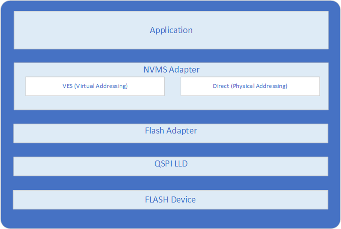
Figure 39 NVMS Overview
In theory NVMS is interface agnostic, as it is independent from the interface type being used (Standard SPI, I2C or QuadSPI) for data storage. However, the QSPI interface is a special interface from the NVMS perspective. As well as performing eXecution in Place (XiP), the QSPI Controller hardware block is also handling specific Flash-aware actions when Flash devices Read/Write/Erase operations are executed. As shown in Figure 41 when DA1469x is in cached mode, special mechanisms from the QSPI block are invoked.
The main consequence of this approach is that all Flash memory models used when utilizing NVMS over QSPI in cached mode must support Erase suspend/resume.
The rest of this section gives an overview on:
Common NVMS interface for all usage scenarios
Mechanisms implemented specifically for NVMS over QSPI in cached mode usage scenario
Virtual EEPROM (VES) emulation
Flash Memory Map in various usage scenarios.
4.2.4.1.2. Interface
To enable the NVMS adapter, both dg_configNVMS_ADAPTER and dg_configFLASH_ADAPTER macros must be defined and set to 1 in the project’s custom
header file, e.g config/custom_config_qspi.h. From this point and on, the adapter services become available.
#define dg_configNVMS_ADAPTER         (1)

#define dg_configFLASH_ADAPTER        (1)
NVMS Adapter exposes functions: ad_nvms_init(), ad_nvms_open(),
ad_nvms_write() and ad_nvms_read(), ad_nvms_erase(). Function
ad_nvms_init() must be called once at platform start to perform all
necessary initialization routines, including discovering underlying
storage partitions. The Application must open one of the partitions
before any read or write activity can be performed. If several partitions are stored on one physical device (i.e. SPI Flash), opening one partition will limit read and writes to this partition only, making all addressing relative to beginning of that partition and not the whole flash. After opening, each partition is accessed in same way, but the exact way that data is stored depends on partition type. Only in the Virtual EEPROM (VES) partition do all reads and writes use virtual addresses that are independent of actual flash location.
nvms_t ad_nvms_open(nvms_partition_id_t id);

for (;;) {

/* addr is any address in partition address space
 * buf can be any address in memory including QSPI mapped flash */

ad_nvms_read(part, addr, buf, sizeof(buf));

ad_nvms_write(part, addr, buf, sizeof(buf));

}
Function ad_nvms_open() can be called many times since it does not
allocate any resources.
Function ad_nvms_read() can be called with any address within the
partition. If address is outside the partition boundaries
ad_nvms_read() will return 0. If the address is inside the partition
but the size would exceed the partition boundary only the data from
within the partition will be accessed.
Function ad_nvms_write() can be called with any address inside
partition address space.
How read or write actually work depends on the accessing method. In the current version of the platform, two accessing methods are supported: (a) Direct Access and (b) VES.
Direct Access
Direct access driver uses the relative address from the beginning of the partition but apart from this there is no address translation. Writes are performed exactly at requested addresses. If write would not change data (same data written) it will not be performed at all. If write can be performed without erasing it will be executed. If write can’t be performed without an erase, then the erase is also initiated. Currently the direct driver does not support caching so writing small pieces of data on an already used sector will trigger many erase operations. If a small write is required for some reason, then ad_nvms_erase() should be called explicitly before each write for efficiency reasons. Power failure during write or erase will result in data loss including data that was not touched by the last write. For power fail safe operation the VES partition should be used.
VES
For an application to use VES there are two prerequisites:
The Partition ID should only be
NVMS_GENERIC_PART.dg_configNVMS_VESvariable should be defined.
VES driver provides access to the partition with power failure protection. It uses virtual addressing. The address space available for the user application is smaller than physical flash space occupied by the partition, but user can read and write to this address space without worrying that data will be lost. If power fails during a write, the specific data being written can be lost but other data will not be affected.
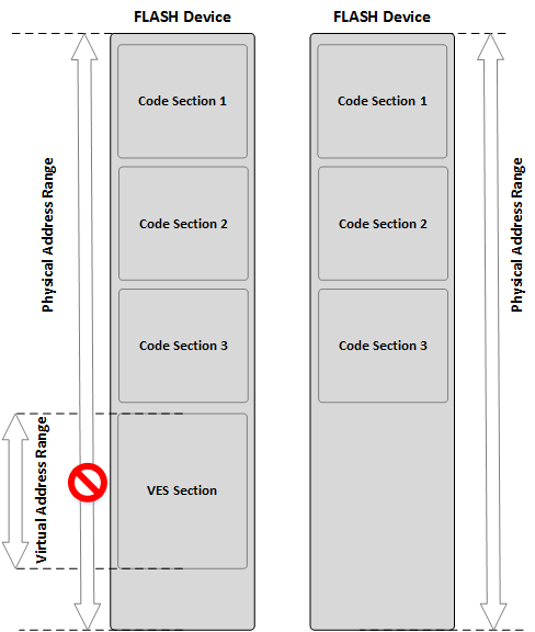
Figure 40 Virtual/Physical Addressing with and without VES
When VES is used:
The application configures NVMS with the VES section information. The VES section is represented by a virtual address range that is mapped to a physical address range.
NVMS prevents the application from performing “raw” writes to the allocated VES section
4.2.4.1.3. NVMS partition table
Code 30 shows the full list of the NVMS IDs and it can be found in
<SDK_ROOT_PATH>/sdk/middleware/adapters/include/partition_def.h
/**
* \brief NVMS Partition IDs
*/
typedef enum {
NVMS_FIRMWARE_PART              = 1,
NVMS_PARAM_PART                 = 2,
NVMS_BIN_PART                   = 3,
NVMS_LOG_PART                   = 4,
NVMS_GENERIC_PART               = 5,
NVMS_PLATFORM_PARAMS_PART       = 15,
NVMS_PARTITION_TABLE            = 16,
NVMS_FW_EXEC_PART               = 17,
NVMS_FW_UPDATE_PART             = 18,
NVMS_PRODUCT_HEADER_PART        = 19,
NVMS_IMAGE_HEADER_PART          = 20,
} nvms_partition_id_t;
Code 31 shows the format for the data of the NVMS.
/**
 * \brief Partition entry.
 */
typedef struct partition_entry_t {
uint8_t magic;          /**< Partition magic number 0xEA */
uint8_t type;           /**< Partition ID */
uint8_t valid;          /**< Valid marker 0xFF */
uint8_t flags;          /**< */
uint16_t start_sector;  /**< Partition start sector */
uint16_t sector_count;  /**< Number of sectors in partition */
uint8_t reserved2[8];   /**< Reserved for future use */
} partition_entry_t;
Magic code (1 byte) |
Partition ID (1 byte) |
Valid flag (1 byte) |
Flags (1 byte) |
Start sector of partition (2 bytes) |
Sector count of partition (2 bytes) |
Reserve (8 bytes) |
|---|---|---|---|---|---|---|
0xEA |
0xFF means it’s an invalid partition entry.
See |
0xFF means it’s a valid partition entry. |
|
Start sector in flash of this partition. |
Sector count of this partition. |
For future use. |
4.2.4.1.4. NVMS over QSPI in cached mode

Figure 41 NVMS Adapter NVMS over QSPI and Virtual EEPROM emulation in Cached mode
When executing in place (XiP) from Flash in cached mode, the Flash device is used to store both firmware images and data.
Preemptive RTOS scheduling remains operational while programming the Flash.
PROGRAM and ERASE are the 2 critical Flash operations triggered by NVMS that need to be considered, as they can’t be performed at the same time as the READ operations triggered by the cache controller when it fetches cache lines from the FLASH to the cache RAM. To handle this conflict a specific mechanism is needed.
This mechanism is disabled when DA1469x is not in cached mode.
4.2.4.1.5. Slice PROGRAM operation
When writing a buffer to the Flash, the NVMS Adapter will slice the buffer into several smaller buffers and will issue several uninterruptible PROGRAM QSPI requests. Note that one parameter determining the size of the slice in bytes is stored in the flash itself. This parameter is determined by:
The interrupt latency time in microseconds that the application authorizes.
The flash model and the time taken to perform a program.
In general, the first byte to be programmed takes longer than the subsequent bytes so a trade-off is possible and the exact value is left to the application developer. However, a default value of 16 bytes is currently used.
4.2.4.1.6. Suspend/Resume ERASE Operation
Instead of slicing ERASE, the DA1469x SDK leverages from Smartbond™ QSPI Controller SUSPEND/ERASE in auto-mode capability. It is assumed here that all selected Flash models support suspending ERASE.

Figure 42 Suspend/Resume ERASE Operation
When requested to erase a sector by NVMS Adapter (staying in auto-mode), the QSPIC will automatically suspend the Erasing operation when a “read” from the Cache controller is triggered due to a miss hit. Two parameters to be stored in the flash itself are SW configurable:
ERASE/RESUME Hold: Refers to
QSPIC_ERASECMDB_REG[QSPIC_ERSRES_HLD]RESUME/SUSPEND delay: Refers to
QSPIC_ERASECMDB_REG[QSPIC_RESSUS_DLY]
As QSPIC is not firing any interrupt on Erase completion, NVMS adapter
must poll QSPIC_ERASECTRL_CMD.
A detailed analysis of the Suspend/Resume ERASE Operation is shown in
Figure 42. The overall process begins when the Application/OS issues an
“Erase Command” Request. The NVMS Adapter receives the Request and
issues an “Erase Sector” Request to the QSPIC (Set QSPIC_ERASECTRL_REC [QSPIC_ERASE_EN]). This request changes the QSPIC state (Figure 42,
Reference Point 1), which checks whether the Flash Memory is idle for
a certain number of Clock Cycles before initiating the ERASE process
(QSPIC_ERASECMDB_REC [QSPIC_ERSRES_HLD]). Provided that the process
can be initiated, QSPIC issues an “Erase Sector” Request to the Flash
Memory and erasing begins. In the meantime, NVMS adapter also switches
state, by writing CHECK_ERASE_REG and ERASECTRL_REQ bits (Figure 42,
Reference Point 2). The Erase process taking place in the Flash Memory,
is able to be suspended by the QSPIC via an “Erase Suspend” Request
in two cases (i) if a Cache Miss Notification arrives in the Cache
control, leading to a “Fetch cache – Read” Request towards the QSPIC and
(ii) if a Read Request is issued by the Application/OS directly to the
QSPIC. The consequent “Erase Suspend” Request initiates the READ process
shown in Figure 42, where QSPIC reads data from the Flash Memory and
issues a “Read Done” Response to (i) Cache Control or (ii)
Application/OS respectively. Then, the QSPIC state switches again,
intending to resume Flash erase if memory is idle for a certain number
of Clock Cycles (QSPIC_ERASECMDB_REG [QSPIC_ERSRES_HLD]) as shown in
Figure 42, Reference Point 3. Provided that the Flash erase can be
resumed, QSPIC issues an “Erase Resume” Request towards the Flash Memory
and changes state once more. In its current state (Figure 42, Reference
Point 4) QPSIC is programmed to delay any new suspension of the
newly-resumed Erase for a pre-defined number of Clock Cycles
(QSPIC_ERASECMDB_REG [QSPIC_RESSUS_DLY]). In the meantime, Flash
Memory concludes the erasing process and notifies the QSPIC with an
“Erase Complete” Response. QSPIC then issues an “Erase Complete”
Response to the NVMS adapter, changing its state thus clearing
CHECK_ERASE_REG and ERASECTRL_REQ bits (Figure 42, Reference Point
5). Finally, NVMS Adapter issues the conclusive “Erase Complete”
Response to the Application/OS.