2. SDADC Adapters Concept
This section explains the procedure to enable and correctly configure the peripheral adapters for SDADC functionality. The procedure is a three-step process which can be applied to almost every type of adapter including serial peripheral adapters (I²C, SPI, UART).
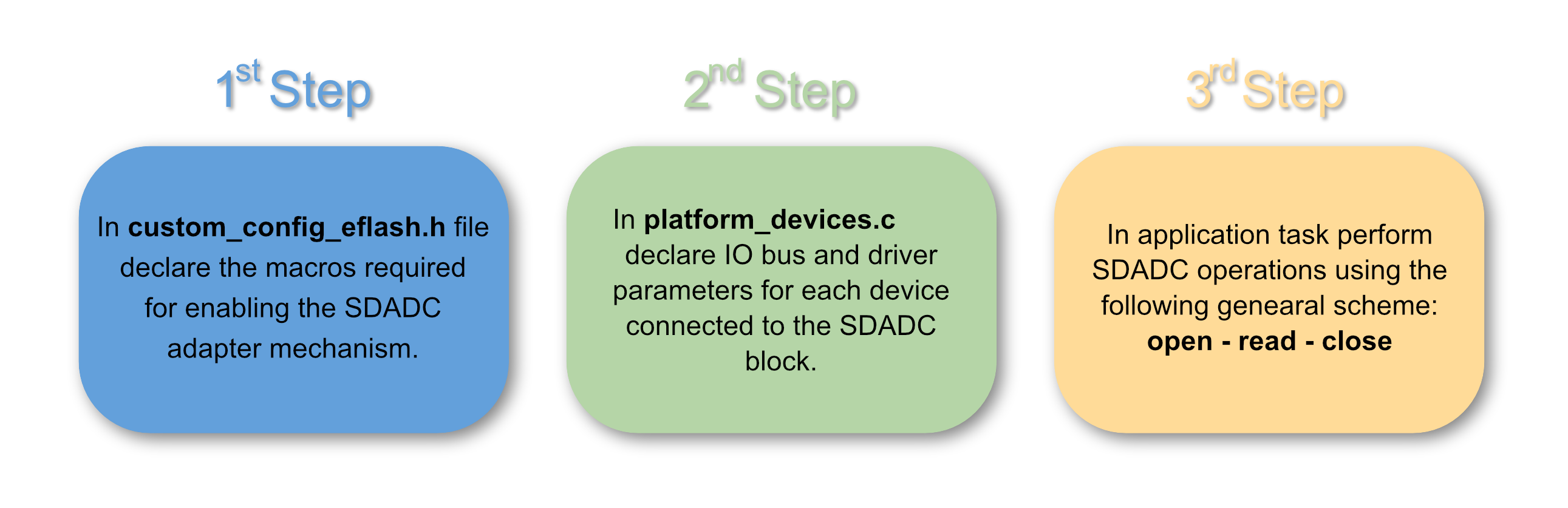
Figure 1 The Three-Step Process for Setting the SDADC Adapter Mechanism
2.1. Preparing the SDADC Adapter
The first step for configuring the SDADC adapter mechanism is to enable it by defining the following macros in
/config/custom_config_xxx.hfile:
/*
 * Macros for enabling SDADC operations using Adapters
 */
#define dg_configSDADC_ADAPTER                    (1)
#define dg_configSDADC_DMA_SUPPORT                (0) // not using DMA by default
From this point onwards, the overall adapter implementation with all its integrated functions is available.
The second step is to declare IO bus as well as driver configurations for all the analog devices connected on the SDADC block. These settings are applied every time the analog device is selected and used. All the configurations should be placed in
platform_devices.cfile.Once the SDADC adapter mechanism is enabled, the developer can use all the available APIs for performing SDADC operations. The following steps describe the required sequence of APIs in an application to successfully execute a SDADC operation.
ad_sdadc_io_config()This must be called once at either platform start (
system_init()) or task initialization to perform all the necessary SDADC initialization routines. For internal Vbat voltage detecting, the IO configuration is not needed.ad_sdadc_open()Before using the SDADC interface, the application task must open the device that will access the SDADC block. Opening a device involves acquiring all the required resources as well as configuring the SDADC controller with the target device and IO bus settings. This function returns a handler to the main flow for use in subsequent adapter functions. Note that this function will block until it acquires all controller resources.
Perform a write/read transaction either synchronously or asynchronously.
After opening a device, the application task can perform any SDADC operation either synchronously or asynchronously. In synchronous mode, the calling task is blocked for the duration of the SDADC operation but other tasks are not. In asynchronous mode, the calling task is not blocked by the SDADC operation and thus the application task can continue with other operations while waiting for a user-defined callback function to be called, signaling the completion of the SDADC operation.
User-defined callback functions are called from within Interrupt Service Routine (ISR) context. Therefore, callback’s execution time should be as short as possible and not contain complex calculations. Please note that for as long as a system interrupt is serviced, the main application is halted.
Do not call asynchronous related APIs consecutively without guaranteeing that the previous asynchronous transaction is finished.
ad_sdadc_close()After all user operations are done and the device is no longer needed, it should be closed. This step involves disabling and de-initializing the SDADC block used as well as releasing all the previously acquired resources.
Note
For more detailed information on the SDADC APIs please refer to sdk\adapters\include\ad_sdadc.h file.
2.2. Handling ADC Measurements
This section describes the basic operation principles of the ADC controller and how to handle the resulting data upon a successful analog-to-digital conversion.
Consider an ADC controller with a voltage reference of 0.9V (Using internal Vref=0.9v) and 15bits LSB, OSR=1024, that is, it has the ability to detect 32767 discrete analog levels. In this case, any analog value in between 0 V and 0.9 V is converted into its equivalent ADC value as shown in Figure 2. The 0 V to 0.9 V range is divided into 215 = 32767 steps. Thus, a 0 V input results in an ADC output of 0, a 0.9 V input results in an ADC output of 32767.
Note
The sigma-delta filter delivers a 16-bit word on a 1 kHz rate. Note that, out of the 16 bits, the 2.5 LSBs are considered to be noise and should be discarded (ENOB = 12.5). More details please refer to the datasheet section 22.2.
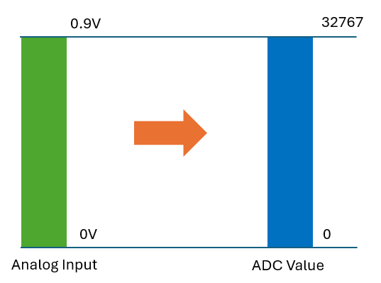
Figure 2 Analog-to-Digital Conversion Process
Figure 3 depicts the relationship between analog and raw ADC values.

Figure 3 Basic Relationship between Analog and Raw ADC Values
Following is an example which demonstrates the computation of the raw ADC value for Vbat/4 (3008/4=752 mV). As described, the ADC voltage reference can be the default 0.9 V. in Figure 4
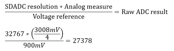
Figure 4 Resulting Raw ADC Value